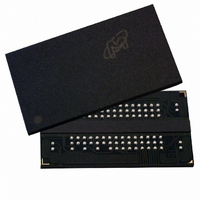
MT47H256M4BT-5E:A TR Micron Technology Inc, MT47H256M4BT-5E:A TR Datasheet - Page 90

MT47H256M4BT-5E:A TR
Manufacturer Part Number
MT47H256M4BT-5E:A TR
Description
IC DDR2 SDRAM 1GBIT 5NS 92FBGA
Manufacturer
Micron Technology Inc
Datasheet
1.MT47H256M4HQ-5EE_TR.pdf
(131 pages)
Specifications of MT47H256M4BT-5E:A TR
Format - Memory
RAM
Memory Type
DDR2 SDRAM
Memory Size
1G (256M x 4)
Speed
5ns
Interface
Parallel
Voltage - Supply
1.7 V ~ 1.9 V
Operating Temperature
0°C ~ 85°C
Package / Case
92-FBGA
Lead Free Status / RoHS Status
Lead free / RoHS Compliant
Other names
557-1206-1
- Current page: 90 of 131
- Download datasheet (10Mb)
READ
PDF: 09005aef821ae8bf
1GbDDR2.pdf – Rev. T 02/10 EN
READ bursts are initiated with a READ command. The starting column and bank ad-
dresses are provided with the READ command, and auto precharge is either enabled or
disabled for that burst access. If auto precharge is enabled, the row being accessed is
automatically precharged at the completion of the burst. If auto precharge is disabled,
the row will be left open after the completion of the burst.
During READ bursts, the valid data-out element from the starting column address will
be available READ latency (RL) clocks later. RL is defined as the sum of AL and CL:
RL = AL + CL. The value for AL and CL are programmable via the MR and EMR com-
mands, respectively. Each subsequent data-out element will be valid nominally at the
next positive or negative clock edge (at the next crossing of CK and CK#). Figure 45
(page 91) shows examples of RL based on different AL and CL settings.
DQS/DQS# is driven by the DDR2 SDRAM along with output data. The initial LOW state
on DQS and the HIGH state on DQS# are known as the read preamble (
LOW state on DQS and the HIGH state on DQS# coincident with the last data-out ele-
ment are known as the read postamble (
Upon completion of a burst, assuming no other commands have been initiated, the DQ
will go High-Z. A detailed explanation of
window hold), and the valid data window are depicted in Figure 54 (page 99) and Fig-
ure 55 (page 100). A detailed explanation of
t
Data from any READ burst may be concatenated with data from a subsequent READ
command to provide a continuous flow of data. The first data element from the new
burst follows the last element of a completed burst. The new READ command should
be issued x cycles after the first READ command, where x equals BL/2 cycles (see Fig-
ure 46 (page 92)).
Nonconsecutive read data is illustrated in Figure 47 (page 93). Full-speed random
read accesses within a page (or pages) can be performed. DDR2 SDRAM supports the
use of concurrent auto precharge timing (see Table 41 (page 96)).
DDR2 SDRAM does not allow interrupting or truncating of any READ burst using BL = 4
operations. Once the BL = 4 READ command is registered, it must be allowed to com-
plete the entire READ burst. However, a READ (with auto precharge disabled) using BL
= 8 operation may be interrupted and truncated only by another READ burst as long as
the interruption occurs on a 4-bit boundary due to the 4n prefetch architecture of
DDR2 SDRAM. As shown in Figure 48 (page 94), READ burst BL = 8 operations may
not be interrupted or truncated with any other command except another READ com-
mand.
Data from any READ burst must be completed before a subsequent WRITE burst is al-
lowed. An example of a READ burst followed by a WRITE burst is shown in Figure 49
(page 94). The
fined in Figure 57 (page 103)).
AC (data-out transition skew to CK) is shown in Figure 56 (page 101).
t
DQSS (NOM) case is shown (
90
Micron Technology, Inc. reserves the right to change products or specifications without notice.
t
t
RPST).
DQSQ (valid data-out skew),
t
t
DQSCK (DQS transition skew to CK) and
DQSS [MIN] and
1Gb: x4, x8, x16 DDR2 SDRAM
© 2004 Micron Technology, Inc. All rights reserved.
t
DQSS [MAX] are de-
t
QH (data-out
t
RPRE). The
READ
Related parts for MT47H256M4BT-5E:A TR
Image
Part Number
Description
Manufacturer
Datasheet
Request
R

Part Number:
Description:
IC DDR2 SDRAM 1GBIT 92FBGA
Manufacturer:
Micron Technology Inc
Datasheet:

Part Number:
Description:
IC DDR2 SDRAM 1GBIT 3NS 92FBGA
Manufacturer:
Micron Technology Inc
Datasheet:

Part Number:
Description:
IC DDR2 SDRAM 1GBIT 5NS 92FBGA
Manufacturer:
Micron Technology Inc
Datasheet:

Part Number:
Description:
IC SDRAM 64MBIT 133MHZ 54TSOP
Manufacturer:
Micron Technology Inc
Datasheet:

Part Number:
Description:
IC SDRAM 64MBIT 5.5NS 86TSOP
Manufacturer:
Micron Technology Inc
Datasheet:

Part Number:
Description:
IC SDRAM 64MBIT 200MHZ 86TSOP
Manufacturer:
Micron Technology Inc
Datasheet:

Part Number:
Description:
IC SDRAM 64MBIT 133MHZ 54TSOP
Manufacturer:
Micron Technology Inc
Datasheet:

Part Number:
Description:
IC SDRAM 128MBIT 133MHZ 54TSOP
Manufacturer:
Micron Technology Inc
Datasheet:

Part Number:
Description:
IC SDRAM 256MBIT 133MHZ 90VFBGA
Manufacturer:
Micron Technology Inc
Datasheet:

Part Number:
Description:
IC SDRAM 128MBIT 133MHZ 54TSOP
Manufacturer:
Micron Technology Inc
Datasheet:

Part Number:
Description:
IC SDRAM 256MBIT 133MHZ 54TSOP
Manufacturer:
Micron Technology Inc
Datasheet:

Part Number:
Description:
IC DDR SDRAM 512MBIT 6NS 66TSOP
Manufacturer:
Micron Technology Inc
Datasheet:

Part Number:
Description:
IC SDRAM 128MBIT 167MHZ 86TSOP
Manufacturer:
Micron Technology Inc
Datasheet:

Part Number:
Description:
IC SDRAM 128MBIT 143MHZ 86TSOP
Manufacturer:
Micron Technology Inc
Datasheet:

Part Number:
Description:
SDRAM 256M-BIT 1.8V 54-PIN VFBGA
Manufacturer:
Micron Technology Inc
Datasheet:


