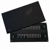
MT47H256M4BT-5E:A TR Micron Technology Inc, MT47H256M4BT-5E:A TR Datasheet - Page 81

MT47H256M4BT-5E:A TR
Manufacturer Part Number
MT47H256M4BT-5E:A TR
Description
IC DDR2 SDRAM 1GBIT 5NS 92FBGA
Manufacturer
Micron Technology Inc
Datasheet
1.MT47H256M4HQ-5EE_TR.pdf
(131 pages)
Specifications of MT47H256M4BT-5E:A TR
Format - Memory
RAM
Memory Type
DDR2 SDRAM
Memory Size
1G (256M x 4)
Speed
5ns
Interface
Parallel
Voltage - Supply
1.7 V ~ 1.9 V
Operating Temperature
0°C ~ 85°C
Package / Case
92-FBGA
Lead Free Status / RoHS Status
Lead free / RoHS Compliant
Other names
557-1206-1
On-Die Termination (ODT)
Off-Chip Driver (OCD) Impedance Calibration
Posted CAS Additive Latency (AL)
PDF: 09005aef821ae8bf
1GbDDR2.pdf – Rev. T 02/10 EN
ODT effective resistance, R
Figure 37 (page 79). The ODT feature is designed to improve signal integrity of the mem-
ory channel by allowing the DDR2 SDRAM controller to independently turn on/off ODT
for any or all devices. R
ble and apply to each DQ, DQS/DQS#, RDQS/RDQS#, UDQS/UDQS#, LDQS/LDQS#,
DM, and UDM/LDM signals. Bits (E6, E2) determine what ODT resistance is enabled by
turning on/off “sw1,” “sw2,” or “sw3.” The ODT effective resistance value is selected by
enabling switch “sw1,” which enables all R1 values that are 150Ω each, enabling an ef-
fective resistance of 75Ω (R
that are 300Ω each, enable an effective ODT resistance of 150Ω (R
Switch “sw3” enables R1 values of 100Ω, enabling effective resistance of 50Ω. Reserved
states should not be used, as an unknown operation or incompatibility with future ver-
sions may result.
The ODT control ball is used to determine when R
ODT has been enabled via bits E2 and E6 of the EMR. The ODT feature and ODT input
ball are only used during active, active power-down (both fast-exit and slow-exit
modes), and precharge power-down modes of operation.
ODT must be turned off prior to entering self refresh mode. During power-up and initi-
alization of the DDR2 SDRAM, ODT should be disabled until the EMR command is
issued. This will enable the ODT feature, at which point the ODT ball will determine the
R
HIGH until eight clocks after the EMR has been enabled (see Figure 80 (page 126) for
ODT timing diagrams).
The OFF-CHIP DRIVER function is an optional DDR2 JEDEC feature not supported by
Micron and thereby must be set to the default state. Enabling OCD beyond the default
settings will alter the I/O drive characteristics and the timing and output I/O specifica-
tions will no longer be valid (see Initialization (page 85) for proper setting of OCD
defaults).
Posted CAS additive latency (AL) is supported to make the command and data bus effi-
cient for sustainable bandwidths in DDR2 SDRAM. Bits E3–E5 define the value of AL, as
shown in Figure 37. Bits E3–E5 allow the user to program the DDR2 SDRAM with an AL
of 0, 1, 2, 3, 4, 5, or 6 clocks. Reserved states should not be used as an unknown opera-
tion or incompatibility with future versions may result.
In this operation, the DDR2 SDRAM allows a READ or WRITE command to be issued
prior to
using this feature would set AL =
is held for the time of the AL before it is issued internally to the DDR2 SDRAM device.
RL is controlled by the sum of AL and CL; RL = AL + CL. WRITE latency (WL) is equal to
RL minus one clock; WL = AL + CL - 1 ×
(page 82). An example of a WL is shown in Figure 39 (page 82).
TT(EFF)
value. Anytime the EMR enables the ODT function, ODT may not be driven
t
RCD (MIN) with the requirement that AL ≤
TT
effective resistance values of 50Ω, 75Ω, and 150Ω are selecta-
TT(EFF)
TT2 [EFF]
81
t
, is defined by bits E2 and E6 of the EMR, as shown in
RCD (MIN) - 1 ×
= R2/2). Similarly, if “sw2” is enabled, all R2 values
Micron Technology, Inc. reserves the right to change products or specifications without notice.
t
CK. An example of RL is shown in Figure 38
Extended Mode Register (EMR)
1Gb: x4, x8, x16 DDR2 SDRAM
TT(EFF)
t
CK. The READ or WRITE command
t
RCD (MIN). A typical application
is turned on and off, assuming
© 2004 Micron Technology, Inc. All rights reserved.
TT2[EFF]
= R2/2).


