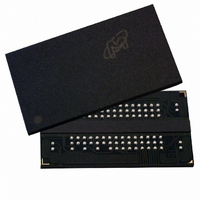
MT47H256M4BT-5E:A TR Micron Technology Inc, MT47H256M4BT-5E:A TR Datasheet - Page 94

MT47H256M4BT-5E:A TR
Manufacturer Part Number
MT47H256M4BT-5E:A TR
Description
IC DDR2 SDRAM 1GBIT 5NS 92FBGA
Manufacturer
Micron Technology Inc
Datasheet
1.MT47H256M4HQ-5EE_TR.pdf
(131 pages)
Specifications of MT47H256M4BT-5E:A TR
Format - Memory
RAM
Memory Type
DDR2 SDRAM
Memory Size
1G (256M x 4)
Speed
5ns
Interface
Parallel
Voltage - Supply
1.7 V ~ 1.9 V
Operating Temperature
0°C ~ 85°C
Package / Case
92-FBGA
Lead Free Status / RoHS Status
Lead free / RoHS Compliant
Other names
557-1206-1
- Current page: 94 of 131
- Download datasheet (10Mb)
Figure 48: READ Interrupted by READ
Figure 49: READ-to-WRITE
READ with Precharge
PDF: 09005aef821ae8bf
1GbDDR2.pdf – Rev. T 02/10 EN
DQS, DQS#
DQS, DQS#
Command
Command
Address
CK#
A10
CK#
DQ
DQ
CK
CK
READ 1
Valid 4
ACT n
T0
T0
Notes:
Notes:
READ n
T1
t CCD
NOP 2
T1
CL = 3 (AL = 0)
t RCD = 3
A READ burst may be followed by a PRECHARGE command to the same bank, provided
auto precharge is not activated. The minimum READ-to-PRECHARGE command spac-
ing to the same bank has two requirements that must be satisfied: AL + BL/2 clocks and
t
prefetch of a READ command to the PRECHARGE command. For BL = 4, this is the time
from the actual READ (AL after the READ command) to PRECHARGE command. For
BL = 8, this is the time from AL + 2 × CK after the READ-to-PRECHARGE command.
Following the PRECHARGE command, a subsequent command to the same bank can-
RTP.
1. BL = 8 required; auto precharge must be disabled (A10 = LOW).
2. NOP or COMMAND INHIBIT commands are valid. PRECHARGE command cannot be is-
3. Interrupting READ command must be issued exactly 2 ×
4. READ command can be issued to any valid bank and row address (READ command at T0
5. Auto precharge can be either enabled (A10 = HIGH) or disabled (A10 = LOW) by the in-
6. Example shown uses AL = 0; CL = 3, BL = 8, shown with nominal
1. BL = 4; CL = 3; AL = 2.
2. Shown with nominal
AL = 2
NOP
T2
sued to banks used for READs at T0 and T2.
and T2 can be either same bank or different bank).
terrupting READ command.
t
READ 3
Valid 5
Valid 4
RTP is the minimum time from the rising clock edge that initiates the last 4-bit
T2
NOP
T3
RL = 5
NOP 2
T3
CL = 3 (AL = 0)
DO
NOP
T4
CL = 3
DO
t
AC,
Valid
T4
WRITE
DO
94
t
T5
DQSCK, and
DO
Valid
T5
NOP
T6
Micron Technology, Inc. reserves the right to change products or specifications without notice.
DO
DO
n
t
DQSQ.
n + 1
DO
WL = RL - 1 = 4
DO
NOP
Valid
T7
1Gb: x4, x8, x16 DDR2 SDRAM
T6
n + 2
DO
DO
n + 3
DO
DO
NOP
T8
Valid
T7
t
CK from previous READ.
DO
Transitioning Data
Transitioning Data
© 2004 Micron Technology, Inc. All rights reserved.
NOP
T9
DI
n
DO
t
AC,
Valid
T8
n + 1
DI
DO
t
DQSCK, and
NOP
T10
n + 2
DI
DO
n + 3
Valid
DI
T9
Don’t Care
Don’t Care
NOP
T11
READ
t
DQSQ.
Related parts for MT47H256M4BT-5E:A TR
Image
Part Number
Description
Manufacturer
Datasheet
Request
R

Part Number:
Description:
IC DDR2 SDRAM 1GBIT 92FBGA
Manufacturer:
Micron Technology Inc
Datasheet:

Part Number:
Description:
IC DDR2 SDRAM 1GBIT 3NS 92FBGA
Manufacturer:
Micron Technology Inc
Datasheet:

Part Number:
Description:
IC DDR2 SDRAM 1GBIT 5NS 92FBGA
Manufacturer:
Micron Technology Inc
Datasheet:

Part Number:
Description:
IC SDRAM 64MBIT 133MHZ 54TSOP
Manufacturer:
Micron Technology Inc
Datasheet:

Part Number:
Description:
IC SDRAM 64MBIT 5.5NS 86TSOP
Manufacturer:
Micron Technology Inc
Datasheet:

Part Number:
Description:
IC SDRAM 64MBIT 200MHZ 86TSOP
Manufacturer:
Micron Technology Inc
Datasheet:

Part Number:
Description:
IC SDRAM 64MBIT 133MHZ 54TSOP
Manufacturer:
Micron Technology Inc
Datasheet:

Part Number:
Description:
IC SDRAM 128MBIT 133MHZ 54TSOP
Manufacturer:
Micron Technology Inc
Datasheet:

Part Number:
Description:
IC SDRAM 256MBIT 133MHZ 90VFBGA
Manufacturer:
Micron Technology Inc
Datasheet:

Part Number:
Description:
IC SDRAM 128MBIT 133MHZ 54TSOP
Manufacturer:
Micron Technology Inc
Datasheet:

Part Number:
Description:
IC SDRAM 256MBIT 133MHZ 54TSOP
Manufacturer:
Micron Technology Inc
Datasheet:

Part Number:
Description:
IC DDR SDRAM 512MBIT 6NS 66TSOP
Manufacturer:
Micron Technology Inc
Datasheet:

Part Number:
Description:
IC SDRAM 128MBIT 167MHZ 86TSOP
Manufacturer:
Micron Technology Inc
Datasheet:

Part Number:
Description:
IC SDRAM 128MBIT 143MHZ 86TSOP
Manufacturer:
Micron Technology Inc
Datasheet:

Part Number:
Description:
SDRAM 256M-BIT 1.8V 54-PIN VFBGA
Manufacturer:
Micron Technology Inc
Datasheet:


