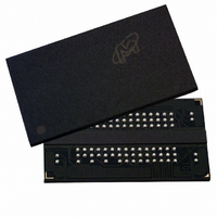
MT47H256M4BT-5E:A TR Micron Technology Inc, MT47H256M4BT-5E:A TR Datasheet - Page 44

MT47H256M4BT-5E:A TR
Manufacturer Part Number
MT47H256M4BT-5E:A TR
Description
IC DDR2 SDRAM 1GBIT 5NS 92FBGA
Manufacturer
Micron Technology Inc
Datasheet
1.MT47H256M4HQ-5EE_TR.pdf
(131 pages)
Specifications of MT47H256M4BT-5E:A TR
Format - Memory
RAM
Memory Type
DDR2 SDRAM
Memory Size
1G (256M x 4)
Speed
5ns
Interface
Parallel
Voltage - Supply
1.7 V ~ 1.9 V
Operating Temperature
0°C ~ 85°C
Package / Case
92-FBGA
Lead Free Status / RoHS Status
Lead free / RoHS Compliant
Other names
557-1206-1
- Current page: 44 of 131
- Download datasheet (10Mb)
Table 16: Differential Input Logic Levels
All voltages referenced to V
Figure 13: Differential Input Signal Levels
PDF: 09005aef821ae8bf
1GbDDR2.pdf – Rev. T 02/10 EN
Parameter
DC input signal voltage
DC differential input voltage
AC differential input voltage
AC differential cross-point voltage
Input midpoint voltage
Notes:
Notes:
SS
V
DDQ
1.075V
0.725V
1. V
2. V
3. V
4. The typical value of V
5. V
6. V
–0.30V
1. TR and CP may not be more positive than V
2. TR represents the CK, DQS, RDQS, LDQS, and UDQS signals; CP represents CK#, DQS#,
3. This provides a minimum of 850mV to a maximum of 950mV and is expected to be
4. TR and CP must cross in this region.
5. TR and CP must meet at least V
6. TR and CP must have a minimum 500mV peak-to-peak swing.
= 1.8V
2.1V
0.9V
CP 2
TR 2
CK#, DQS, DQS#, LDQS, LDQS#, UDQS, UDQS#, and RDQS, RDQS#.
V
input (such as CK#, DQS#, LDQS#, UDQS#) level. The minimum value is equal to V
V
V
mentary input (such as CK#, DQS#, LDQS#, UDQS#, RDQS#) level. The minimum value is
equal to V
and V
differential input signals must cross, as shown in Figure 13.
the true input (CK, DQS) level and V
is expected to be approximately 0.5 × V
RDQS#, LDQS#, and UDQS# signals.
V
IN(DC)
ID(DC)
TR
IL(DC)
ID(AC)
TR
MP(DC)
DDQ
DDQ
is the true input (such as CK, DQS, LDQS, UDQS) level and V
is the true input (such as CK, DQS, LDQS, UDQS, RDQS) level and V
Input Electrical Characteristics and Operating Conditions
/2.
+ 300mV allowed provided 1.9V is not exceeded.
IX(AC)
. Differential input signal levels are shown in Figure 13.
X
specifies the allowable DC execution of each input of differential pair such as CK,
specifies the input differential voltage |V
specifies the input differential voltage |V
specifies the input differential common mode voltage (V
IH(AC)
is expected to track variations in V
Symbol
V
V
V
V
V
MP(DC)
IN(DC)
ID(DC)
ID(AC)
IX(AC)
- V
IL(AC)
IX(AC)
, as shown in Table 15 (page 43).
44
0.50 × V
is expected to be about 0.5 × V
X
ID(DC)min
–300
Min
250
500
850
DDQ
CP
Micron Technology, Inc. reserves the right to change products or specifications without notice.
- 175
is the complementary input (CK#, DQS#). V
DDQ
when static and is centered around V
.
DDQ
1Gb: x4, x8, x16 DDR2 SDRAM
DDQ
+ 0.3V or more negative than V
TR
TR
V
V
V
. V
IN(DC)max
MP(DC)
IN(DC)min
0.50 × V
- V
- V
IX(AC)
3
CP
CP
1
1
V
| required for switching, where
| required for switching, where
IX(AC)
V
V
V
Max
950
indicates the voltage at which
4
DDQ
DDQ
DDQ
DDQ
DDQ
V
ID(DC)
© 2004 Micron Technology, Inc. All rights reserved.
+ 175
of the transmitting device
5
V
CP
ID(AC)
TR
6
is the complementary
+ V
CP
CP
Units
)/2 where V
is the comple-
mV
mV
mV
mV
mV
MP(DC)
SS
Notes
IH(DC)
- 0.3V.
MP(DC)
1, 6
2, 6
3, 6
.
4
5
TR
is
-
Related parts for MT47H256M4BT-5E:A TR
Image
Part Number
Description
Manufacturer
Datasheet
Request
R

Part Number:
Description:
IC DDR2 SDRAM 1GBIT 92FBGA
Manufacturer:
Micron Technology Inc
Datasheet:

Part Number:
Description:
IC DDR2 SDRAM 1GBIT 3NS 92FBGA
Manufacturer:
Micron Technology Inc
Datasheet:

Part Number:
Description:
IC DDR2 SDRAM 1GBIT 5NS 92FBGA
Manufacturer:
Micron Technology Inc
Datasheet:

Part Number:
Description:
IC SDRAM 64MBIT 133MHZ 54TSOP
Manufacturer:
Micron Technology Inc
Datasheet:

Part Number:
Description:
IC SDRAM 64MBIT 5.5NS 86TSOP
Manufacturer:
Micron Technology Inc
Datasheet:

Part Number:
Description:
IC SDRAM 64MBIT 200MHZ 86TSOP
Manufacturer:
Micron Technology Inc
Datasheet:

Part Number:
Description:
IC SDRAM 64MBIT 133MHZ 54TSOP
Manufacturer:
Micron Technology Inc
Datasheet:

Part Number:
Description:
IC SDRAM 128MBIT 133MHZ 54TSOP
Manufacturer:
Micron Technology Inc
Datasheet:

Part Number:
Description:
IC SDRAM 256MBIT 133MHZ 90VFBGA
Manufacturer:
Micron Technology Inc
Datasheet:

Part Number:
Description:
IC SDRAM 128MBIT 133MHZ 54TSOP
Manufacturer:
Micron Technology Inc
Datasheet:

Part Number:
Description:
IC SDRAM 256MBIT 133MHZ 54TSOP
Manufacturer:
Micron Technology Inc
Datasheet:

Part Number:
Description:
IC DDR SDRAM 512MBIT 6NS 66TSOP
Manufacturer:
Micron Technology Inc
Datasheet:

Part Number:
Description:
IC SDRAM 128MBIT 167MHZ 86TSOP
Manufacturer:
Micron Technology Inc
Datasheet:

Part Number:
Description:
IC SDRAM 128MBIT 143MHZ 86TSOP
Manufacturer:
Micron Technology Inc
Datasheet:

Part Number:
Description:
SDRAM 256M-BIT 1.8V 54-PIN VFBGA
Manufacturer:
Micron Technology Inc
Datasheet:


