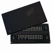
MT47H256M4BT-5E:A TR Micron Technology Inc, MT47H256M4BT-5E:A TR Datasheet - Page 80

MT47H256M4BT-5E:A TR
Manufacturer Part Number
MT47H256M4BT-5E:A TR
Description
IC DDR2 SDRAM 1GBIT 5NS 92FBGA
Manufacturer
Micron Technology Inc
Datasheet
1.MT47H256M4HQ-5EE_TR.pdf
(131 pages)
Specifications of MT47H256M4BT-5E:A TR
Format - Memory
RAM
Memory Type
DDR2 SDRAM
Memory Size
1G (256M x 4)
Speed
5ns
Interface
Parallel
Voltage - Supply
1.7 V ~ 1.9 V
Operating Temperature
0°C ~ 85°C
Package / Case
92-FBGA
Lead Free Status / RoHS Status
Lead free / RoHS Compliant
Other names
557-1206-1
- Current page: 80 of 131
- Download datasheet (10Mb)
DLL Enable/Disable
Output Drive Strength
DQS# Enable/Disable
RDQS Enable/Disable
Output Enable/Disable
PDF: 09005aef821ae8bf
1GbDDR2.pdf – Rev. T 02/10 EN
The DLL may be enabled or disabled by programming bit E0 during the LM command,
as shown in Figure 37 (page 79). These specifications are applicable when the DLL is
enabled for normal operation. DLL enable is required during power-up initialization
and upon returning to normal operation after having disabled the DLL for the purpose
of debugging or evaluation. Enabling the DLL should always be followed by resetting
the DLL using the LM command.
The DLL is automatically disabled when entering SELF REFRESH operation and is auto-
matically re-enabled and reset upon exit of SELF REFRESH operation.
Anytime the DLL is enabled (and subsequently reset), 200 clock cycles must occur be-
fore a READ command can be issued to allow time for the internal clock to synchronize
with the external clock. Failing to wait for synchronization to occur may result in a viola-
tion of the
Anytime the DLL is disabled and the device is operated below 25 MHz, any AUTO RE-
FRESH command should be followed by a PRECHARGE ALL command.
The output drive strength is defined by bit E1, as shown in Figure 37. The normal drive
strength for all outputs is specified to be SSTL_18. Programming bit E1 = 0 selects nor-
mal (full strength) drive strength for all outputs. Selecting a reduced drive strength
option (E1 = 1) will reduce all outputs to approximately 45 to 60 percent of the SSTL_18
drive strength. This option is intended for the support of lighter load and/or point-to-
point environments.
The DQS# ball is enabled by bit E10. When E10 = 0, DQS# is the complement of the
differential data strobe pair DQS/DQS#. When disabled (E10 = 1), DQS is used in a single-
ended mode and the DQS# ball is disabled. When disabled, DQS# should be left float-
ing; however, it may be tied to ground via a 20Ω to 10kΩ resistor. This function is also
used to enable/disable RDQS#. If RDQS is enabled (E11 = 1) and DQS# is enabled (E10 =
0), then both DQS# and RDQS# will be enabled.
The RDQS ball is enabled by bit E11, as shown in Figure 37. This feature is only applica-
ble to the x8 configuration. When enabled (E11 = 1), RDQS is identical in function and
timing to data strobe DQS during a READ. During a WRITE operation, RDQS is ignored
by the DDR2 SDRAM.
The OUTPUT ENABLE function is defined by bit E12, as shown in Figure 37. When ena-
bled (E12 = 0), all outputs (DQ, DQS, DQS#, RDQS, RDQS#) function normally. When
disabled (E12 = 1), all outputs (DQ, DQS, DQS#, RDQS, RDQS#) are disabled, thus remov-
ing output buffer current. The output disable feature is intended to be used during I
characterization of read current.
t
AC or
t
DQSCK parameters.
80
Micron Technology, Inc. reserves the right to change products or specifications without notice.
Extended Mode Register (EMR)
1Gb: x4, x8, x16 DDR2 SDRAM
© 2004 Micron Technology, Inc. All rights reserved.
DD
Related parts for MT47H256M4BT-5E:A TR
Image
Part Number
Description
Manufacturer
Datasheet
Request
R

Part Number:
Description:
IC DDR2 SDRAM 1GBIT 92FBGA
Manufacturer:
Micron Technology Inc
Datasheet:

Part Number:
Description:
IC DDR2 SDRAM 1GBIT 3NS 92FBGA
Manufacturer:
Micron Technology Inc
Datasheet:

Part Number:
Description:
IC DDR2 SDRAM 1GBIT 5NS 92FBGA
Manufacturer:
Micron Technology Inc
Datasheet:

Part Number:
Description:
IC SDRAM 64MBIT 133MHZ 54TSOP
Manufacturer:
Micron Technology Inc
Datasheet:

Part Number:
Description:
IC SDRAM 64MBIT 5.5NS 86TSOP
Manufacturer:
Micron Technology Inc
Datasheet:

Part Number:
Description:
IC SDRAM 64MBIT 200MHZ 86TSOP
Manufacturer:
Micron Technology Inc
Datasheet:

Part Number:
Description:
IC SDRAM 64MBIT 133MHZ 54TSOP
Manufacturer:
Micron Technology Inc
Datasheet:

Part Number:
Description:
IC SDRAM 128MBIT 133MHZ 54TSOP
Manufacturer:
Micron Technology Inc
Datasheet:

Part Number:
Description:
IC SDRAM 256MBIT 133MHZ 90VFBGA
Manufacturer:
Micron Technology Inc
Datasheet:

Part Number:
Description:
IC SDRAM 128MBIT 133MHZ 54TSOP
Manufacturer:
Micron Technology Inc
Datasheet:

Part Number:
Description:
IC SDRAM 256MBIT 133MHZ 54TSOP
Manufacturer:
Micron Technology Inc
Datasheet:

Part Number:
Description:
IC DDR SDRAM 512MBIT 6NS 66TSOP
Manufacturer:
Micron Technology Inc
Datasheet:

Part Number:
Description:
IC SDRAM 128MBIT 167MHZ 86TSOP
Manufacturer:
Micron Technology Inc
Datasheet:

Part Number:
Description:
IC SDRAM 128MBIT 143MHZ 86TSOP
Manufacturer:
Micron Technology Inc
Datasheet:

Part Number:
Description:
SDRAM 256M-BIT 1.8V 54-PIN VFBGA
Manufacturer:
Micron Technology Inc
Datasheet:


