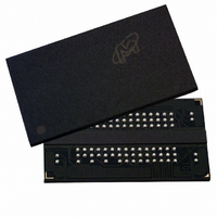
MT47H256M4BT-5E:A TR Micron Technology Inc, MT47H256M4BT-5E:A TR Datasheet - Page 106

MT47H256M4BT-5E:A TR
Manufacturer Part Number
MT47H256M4BT-5E:A TR
Description
IC DDR2 SDRAM 1GBIT 5NS 92FBGA
Manufacturer
Micron Technology Inc
Datasheet
1.MT47H256M4HQ-5EE_TR.pdf
(131 pages)
Specifications of MT47H256M4BT-5E:A TR
Format - Memory
RAM
Memory Type
DDR2 SDRAM
Memory Size
1G (256M x 4)
Speed
5ns
Interface
Parallel
Voltage - Supply
1.7 V ~ 1.9 V
Operating Temperature
0°C ~ 85°C
Package / Case
92-FBGA
Lead Free Status / RoHS Status
Lead free / RoHS Compliant
Other names
557-1206-1
- Current page: 106 of 131
- Download datasheet (10Mb)
Figure 61: WRITE-to-READ
PDF: 09005aef821ae8bf
1GbDDR2.pdf – Rev. T 02/10 EN
Command
DQS, DQS#
DQS, DQS#
DQS, DQS#
t DQSS (NOM)
t DQSS (MIN)
t DQSS (MAX)
Address
CK#
DM
DM
DM
DQ
DQ
DQ
CK
WRITE
Bank a,
Col b
T0
WL - t DQSS
Notes:
WL ± t DQSS
WL + t DQSS
NOP
T1
1.
2. Subsequent rising DQS signals must align to the clock within
3. DI b = data-in for column b; DO n = data-out from column n.
4. BL = 4, AL = 0, CL = 3; thus, WL = 2.
5. One subsequent element of data-in is applied in the programmed order following DI b.
6.
7. A10 is LOW with the WRITE command (auto precharge is disabled).
8. The number of clock cycles required to meet
t
quired between module ranks.
t
greater.
DI
b
WTR is required for any READ following a WRITE to the same device, but it is not re-
WTR is referenced from the first positive CK edge after the last data-in pair.
NOP
T2
DI
b
DI
b
T2n
2
NOP
T3
2
2
T3n
NOP
T4
106
t WTR 1
T5
NOP
Micron Technology, Inc. reserves the right to change products or specifications without notice.
Bank a,
1Gb: x4, x8, x16 DDR2 SDRAM
READ
T6
Col n
t
WTR is either 2 or
CL = 3
CL = 3
CL = 3
T7
NOP
Transitioning Data
© 2004 Micron Technology, Inc. All rights reserved.
t
DQSS.
t
WTR/
T8
NOP
t
CK, whichever is
T9
NOP
Don’t Care
WRITE
DI
DI
DI
T9n
Related parts for MT47H256M4BT-5E:A TR
Image
Part Number
Description
Manufacturer
Datasheet
Request
R

Part Number:
Description:
IC DDR2 SDRAM 1GBIT 92FBGA
Manufacturer:
Micron Technology Inc
Datasheet:

Part Number:
Description:
IC DDR2 SDRAM 1GBIT 3NS 92FBGA
Manufacturer:
Micron Technology Inc
Datasheet:

Part Number:
Description:
IC DDR2 SDRAM 1GBIT 5NS 92FBGA
Manufacturer:
Micron Technology Inc
Datasheet:

Part Number:
Description:
IC SDRAM 64MBIT 133MHZ 54TSOP
Manufacturer:
Micron Technology Inc
Datasheet:

Part Number:
Description:
IC SDRAM 64MBIT 5.5NS 86TSOP
Manufacturer:
Micron Technology Inc
Datasheet:

Part Number:
Description:
IC SDRAM 64MBIT 200MHZ 86TSOP
Manufacturer:
Micron Technology Inc
Datasheet:

Part Number:
Description:
IC SDRAM 64MBIT 133MHZ 54TSOP
Manufacturer:
Micron Technology Inc
Datasheet:

Part Number:
Description:
IC SDRAM 128MBIT 133MHZ 54TSOP
Manufacturer:
Micron Technology Inc
Datasheet:

Part Number:
Description:
IC SDRAM 256MBIT 133MHZ 90VFBGA
Manufacturer:
Micron Technology Inc
Datasheet:

Part Number:
Description:
IC SDRAM 128MBIT 133MHZ 54TSOP
Manufacturer:
Micron Technology Inc
Datasheet:

Part Number:
Description:
IC SDRAM 256MBIT 133MHZ 54TSOP
Manufacturer:
Micron Technology Inc
Datasheet:

Part Number:
Description:
IC DDR SDRAM 512MBIT 6NS 66TSOP
Manufacturer:
Micron Technology Inc
Datasheet:

Part Number:
Description:
IC SDRAM 128MBIT 167MHZ 86TSOP
Manufacturer:
Micron Technology Inc
Datasheet:

Part Number:
Description:
IC SDRAM 128MBIT 143MHZ 86TSOP
Manufacturer:
Micron Technology Inc
Datasheet:

Part Number:
Description:
SDRAM 256M-BIT 1.8V 54-PIN VFBGA
Manufacturer:
Micron Technology Inc
Datasheet:


