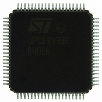
UPSD3433EB40U6 STMicroelectronics, UPSD3433EB40U6 Datasheet - Page 104

UPSD3433EB40U6
Manufacturer Part Number
UPSD3433EB40U6
Description
MCU 8BIT 8032 128KB FLASH 80TQFP
Manufacturer
STMicroelectronics
Series
µPSDr
Datasheet
1.UPSD3434EB40T6.pdf
(293 pages)
Specifications of UPSD3433EB40U6
Core Processor
8032
Core Size
8-Bit
Speed
40MHz
Connectivity
I²C, IrDA, SPI, UART/USART, USB
Peripherals
LVD, POR, PWM, WDT
Number Of I /o
46
Program Memory Size
160KB (160K x 8)
Program Memory Type
FLASH
Ram Size
8K x 8
Voltage - Supply (vcc/vdd)
3 V ~ 5.5 V
Data Converters
A/D 8x10b
Oscillator Type
Internal
Operating Temperature
-40°C ~ 85°C
Package / Case
80-TQFP, 80-VQFP
For Use With
497-5518 - EVAL BOARD RFID READER497-5046 - KIT TOOL FOR ST7/UPSD/STR7 MCU
Lead Free Status / RoHS Status
Lead free / RoHS Compliant
Eeprom Size
-
Other names
497-5660
Available stocks
Company
Part Number
Manufacturer
Quantity
Price
Company:
Part Number:
UPSD3433EB40U6
Manufacturer:
STMicroelectronics
Quantity:
10 000
- Current page: 104 of 293
- Download datasheet (5Mb)
Serial UART interfaces
21.4
104/293
More about UART mode 0
Refer to the block diagram in
page
Transmission is initiated by any instruction which writes to the SFR named SBUF. At the end
of a write operation to SBUF, a 1 is loaded into the 9th position of the transmit shift register
and tells the TX Control unit to begin a transmission. Transmission begins on the following
MCU machine cycle, when the “SEND” signal is active in
SEND enables the output of the shift register to the alternate function on the port containing
pin RxD, and also enables the SHIFT CLOCK signal to the alternate function on the port
containing the pin, TxD. At the end of each SHIFT CLOCK in which SEND is active, the
contents of the transmit shift register are shifted to the right one position.
As data bits shift out to the right, zeros come in from the left. When the MSB of the data byte
is at the output position of the shift register, then the '1' that was initially loaded into the 9th
position, is just to the left of the MSB, and all positions to the left of that contain zeros. This
condition flags the TX Control unit to do one last shift, then deactivate SEND, and then set
the interrupt flag TI. Both of these actions occur at S1P1.
Reception is initiated by the condition REN = 1 and RI = 0. At the end of the next MCU
machine cycle, the RX Control unit writes the bits 11111110 to the receive shift register, and
in the next clock phase activates RECEIVE. RECEIVE enables the SHIFT CLOCK signal to
the alternate function on the port containing the pin, TxD. Each pulse of SHIFT CLOCK
moves the contents of the receive shift register one position to the left while RECEIVE is
active. The value that comes in from the right is the value that was sampled at the RxD pin.
As data bits come in from the right, 1s shift out to the left. When the 0 that was initially
loaded into the right-most position arrives at the left-most position in the shift register, it flags
the RX Control unit to do one last shift, and then it loads SBUF. After this, RECEIVE is
cleared, and the receive interrupt flag RI is set.
Modes 1 or 3
Modes 1 or 3
Modes 1 or 3
Modes 1 or 3
UART Mode
105.
f
OSC
3.6864
3.6864
1.8432
1.8432
MHz
Desired
19200
Baud
9600
9600
4800
Rate
Figure 31 on page
Resultant
19200
Baud
Rate
9600
9600
4800
Deviation
105, and timing diagram in
Baud
Rate
0
0
0
0
Figure
SMOD
PCON
bit in
1
1
1
1
32.
C/T Bit
TMOD
in
0
0
0
0
TMOD
Timer 1
Timer
Mode
Figure 32 on
in
2
2
2
2
uPSD34xx
Reload
value
(hex)
TH1
FE
FE
FF
FF
Related parts for UPSD3433EB40U6
Image
Part Number
Description
Manufacturer
Datasheet
Request
R

Part Number:
Description:
MCU 8BIT 8032 128KB FLASH 80TQFP
Manufacturer:
STMicroelectronics
Datasheet:

Part Number:
Description:
MCU 8BIT 8032 128KB FLASH 52TQFP
Manufacturer:
STMicroelectronics
Datasheet:

Part Number:
Description:
STMicroelectronics [RIPPLE-CARRY BINARY COUNTER/DIVIDERS]
Manufacturer:
STMicroelectronics
Datasheet:

Part Number:
Description:
STMicroelectronics [LIQUID-CRYSTAL DISPLAY DRIVERS]
Manufacturer:
STMicroelectronics
Datasheet:

Part Number:
Description:
BOARD EVAL FOR MEMS SENSORS
Manufacturer:
STMicroelectronics
Datasheet:

Part Number:
Description:
NPN TRANSISTOR POWER MODULE
Manufacturer:
STMicroelectronics
Datasheet:

Part Number:
Description:
TURBOSWITCH ULTRA-FAST HIGH VOLTAGE DIODE
Manufacturer:
STMicroelectronics
Datasheet:

Part Number:
Description:
Manufacturer:
STMicroelectronics
Datasheet:

Part Number:
Description:
DIODE / SCR MODULE
Manufacturer:
STMicroelectronics
Datasheet:

Part Number:
Description:
DIODE / SCR MODULE
Manufacturer:
STMicroelectronics
Datasheet:

Part Number:
Description:
Search -----> STE16N100
Manufacturer:
STMicroelectronics
Datasheet:

Part Number:
Description:
Search ---> STE53NA50
Manufacturer:
STMicroelectronics
Datasheet:


