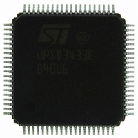
UPSD3433EB40U6 STMicroelectronics, UPSD3433EB40U6 Datasheet - Page 238

UPSD3433EB40U6
Manufacturer Part Number
UPSD3433EB40U6
Description
MCU 8BIT 8032 128KB FLASH 80TQFP
Manufacturer
STMicroelectronics
Series
µPSDr
Datasheet
1.UPSD3434EB40T6.pdf
(293 pages)
Specifications of UPSD3433EB40U6
Core Processor
8032
Core Size
8-Bit
Speed
40MHz
Connectivity
I²C, IrDA, SPI, UART/USART, USB
Peripherals
LVD, POR, PWM, WDT
Number Of I /o
46
Program Memory Size
160KB (160K x 8)
Program Memory Type
FLASH
Ram Size
8K x 8
Voltage - Supply (vcc/vdd)
3 V ~ 5.5 V
Data Converters
A/D 8x10b
Oscillator Type
Internal
Operating Temperature
-40°C ~ 85°C
Package / Case
80-TQFP, 80-VQFP
For Use With
497-5518 - EVAL BOARD RFID READER497-5046 - KIT TOOL FOR ST7/UPSD/STR7 MCU
Lead Free Status / RoHS Status
Lead free / RoHS Compliant
Eeprom Size
-
Other names
497-5660
Available stocks
Company
Part Number
Manufacturer
Quantity
Price
Company:
Part Number:
UPSD3433EB40U6
Manufacturer:
STMicroelectronics
Quantity:
10 000
- Current page: 238 of 293
- Download datasheet (5Mb)
PSD module
Note:
28.5.49
238/293
1
Figure 86. Port B structure
Port pins PB0-PB3 are capable of Fast Slew Rate output drive option. Port pins PB4-PB7
are capable of Open Drain output option.
Port C structure
Port C supports the following operating modes on pins PC2, PC3, PC4, PC7:
●
●
●
See
Port C pins can also be configured in PSDsoft for other dedicated functions:
●
ALLOCATOR
FROM OMC
FROM AND-
INPUT BUS
OR ARRAY
FROM PLD
Figure 87 on page 239
MCU I/O Mode
GPLD Output Mode from Output Macrocells MCELLBC2, MCELLBC3, MCELLBC4,
MCELLBC7
GPLD Input Mode to Input Macrocells IMCC2, IMCC3, IMCC4, IMCC7
Pins PC3 and PC4 support TSTAT and TERR status indicators, to reduce the amount
of time required for JTAG ISP programming. These two pins must be used together for
this function, adding to the four standard JTAG signals. When TSTAT and TERR are
used, it is referred to as “6-pin JTAG”. PC3 and PC4 cannot be used for other functions
8032
8032 RD
PT OUTPUT ENABLE (.OE)
PSD MODULE RESET
DATA
LATCHED ADDR BIT
FROM OMC OUTPUT
(MCELLABx or MCELLBCx)
8032
BITS
WR
DATA
8032
BIT
REGIS-
D
CSIOP
TERS
CLR
M
Q
P
D
B
U
X
Q
Q
Q
REGISTERS
1
2
3
4
5
6
DIRECTION
ONE of 6
CONTROL
DATA OUT
(MCUI/O)
CSIOP
ENABLE OUT
DIRECTION
DRIVE SELECT
CONTROL
DATA OUT
(MCUI/O)
DATA IN (MCUI/O)
DRIVE
RESET
for detail.
TO IMCs
OUTPUT
SELECT
PSDsoft
1
2
3
O
U
U
M
U
T
P
T
X
IMCB0 - IMCB7
DRIVE TYPE SELECT
OUTPUT
ENABLE
OUTPUT
ENABLE
OUTPUT
1 = OPEN
PB4 - PB7
DRAIN,
PIN
NO
HYSTERESIS
BUFFER
CMOS
(1)
1 = FAST
SLEW RATE,
PB0 - PB3
I/O PORT B
PIN INPUT
LOGIC
V
DD
V
DD
uPSD34xx
PIN, PORT B
TYPICAL
AI09180
Related parts for UPSD3433EB40U6
Image
Part Number
Description
Manufacturer
Datasheet
Request
R

Part Number:
Description:
MCU 8BIT 8032 128KB FLASH 80TQFP
Manufacturer:
STMicroelectronics
Datasheet:

Part Number:
Description:
MCU 8BIT 8032 128KB FLASH 52TQFP
Manufacturer:
STMicroelectronics
Datasheet:

Part Number:
Description:
STMicroelectronics [RIPPLE-CARRY BINARY COUNTER/DIVIDERS]
Manufacturer:
STMicroelectronics
Datasheet:

Part Number:
Description:
STMicroelectronics [LIQUID-CRYSTAL DISPLAY DRIVERS]
Manufacturer:
STMicroelectronics
Datasheet:

Part Number:
Description:
BOARD EVAL FOR MEMS SENSORS
Manufacturer:
STMicroelectronics
Datasheet:

Part Number:
Description:
NPN TRANSISTOR POWER MODULE
Manufacturer:
STMicroelectronics
Datasheet:

Part Number:
Description:
TURBOSWITCH ULTRA-FAST HIGH VOLTAGE DIODE
Manufacturer:
STMicroelectronics
Datasheet:

Part Number:
Description:
Manufacturer:
STMicroelectronics
Datasheet:

Part Number:
Description:
DIODE / SCR MODULE
Manufacturer:
STMicroelectronics
Datasheet:

Part Number:
Description:
DIODE / SCR MODULE
Manufacturer:
STMicroelectronics
Datasheet:

Part Number:
Description:
Search -----> STE16N100
Manufacturer:
STMicroelectronics
Datasheet:

Part Number:
Description:
Search ---> STE53NA50
Manufacturer:
STMicroelectronics
Datasheet:


