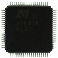
UPSD3433EB40U6 STMicroelectronics, UPSD3433EB40U6 Datasheet - Page 230

UPSD3433EB40U6
Manufacturer Part Number
UPSD3433EB40U6
Description
MCU 8BIT 8032 128KB FLASH 80TQFP
Manufacturer
STMicroelectronics
Series
µPSDr
Datasheet
1.UPSD3434EB40T6.pdf
(293 pages)
Specifications of UPSD3433EB40U6
Core Processor
8032
Core Size
8-Bit
Speed
40MHz
Connectivity
I²C, IrDA, SPI, UART/USART, USB
Peripherals
LVD, POR, PWM, WDT
Number Of I /o
46
Program Memory Size
160KB (160K x 8)
Program Memory Type
FLASH
Ram Size
8K x 8
Voltage - Supply (vcc/vdd)
3 V ~ 5.5 V
Data Converters
A/D 8x10b
Oscillator Type
Internal
Operating Temperature
-40°C ~ 85°C
Package / Case
80-TQFP, 80-VQFP
For Use With
497-5518 - EVAL BOARD RFID READER497-5046 - KIT TOOL FOR ST7/UPSD/STR7 MCU
Lead Free Status / RoHS Status
Lead free / RoHS Compliant
Eeprom Size
-
Other names
497-5660
Available stocks
Company
Part Number
Manufacturer
Quantity
Price
Company:
Part Number:
UPSD3433EB40U6
Manufacturer:
STMicroelectronics
Quantity:
10 000
- Current page: 230 of 293
- Download datasheet (5Mb)
PSD module
Note:
Note:
28.5.38
230/293
2
2
3
1
1
Table 132. MCU I/O mode port C direction register (address = csiop + offset 14h)
For each bit, 1 = out from uPSD34xx port pin1, 0 = in to PSD34xx port pin
Default state for register is 00h after reset or power-up
Table 133. MCU I/O mode port D direction register (address = csiop + offset 15h)
For each bit, 1 = out from uPSD34xx port pin1, 0 = in to PSD34xx port pin
Default state for register is 00h after reset or power-up
Not available on 52-pin uPSD34xx devices
PLD I/O mode
Pins on Ports A, B, C, and D can serve as inputs to either the DPLD or the GPLD. Inputs to
these PLDs from Ports A, B, and C are routed through IMCs before reaching the PLD input
bus. Inputs to the PLDs from Port D do not pass through IMCs, but route directly to the PLD
input bus.
Pins on Ports A, B, and C can serve as outputs from GPLD OMCs, and Port D pins can be
outputs from the DPLD (external chip-selects) which do not consume OMCs.
Whenever a pin is specified to be a PLD output, it cannot be used for MCU I/O mode, or
other pin modes. If a pin is specified to be a PLD input, it is still possible to read the pin using
MCU I/O input mode with the csiop register Data In. Also, the csiop Direction register can
still affect a pin which is used for a PLD input. The csiop Data Out register has no effect on a
PLD output pin.
Each pin on Ports A, B, C, and D have a tri-state buffer at the final output stage. The Output
Enable signal for this buffer is driven by the logical OR of two signals. One signal is an
Output Enable signal generated by the AND-OR array (from an .oe equation specified in
PSDsoft), and the other signal is the output of the csiop Direction register. This logic is
shown in
(Direction registers default to 00h). However, if an equation is written for the Output Enable
that is active at power-on, then the pin will behave as an output.
PLD I/O equations are specified in PSDsoft Express and programmed into the uPSD using
JTAG.
pins of Port B.
To give a general idea of how PLD logic is implemented using PSDsoft Express,
on page 231
output at pin PB0 declared as “Combinatorial” in the “PLD Output” section, and a signal
name, “pld_out”, is specified. The other three signals on pins PB1, PB2, and PB3 would be
declared as “Logic or Address” in the “PLD Input” section, and given signal names.
In the “Design Assistant” window of PSDsoft Express shown in
user simply enters the logic equation for the signal “pld_out” as shown. The user can either
type in the logic statements or enter them using a point-and-click method, selecting various
signal names and logic operators available in the window.
Bit 7
Bit 7
PC7
N/A
Figure 81
Figure 80 on page
illustrates the pin declaration window of PSDsoft Express, showing the PLD
Bit 6
Bit 6
N/A
N/A
shows a very simple combinatorial logic example which is implemented on
Bit 5
Bit 5
N/A
N/A
226. At power-on, all port pins default to high-impedance input
Bit 4
Bit 4
PC4
N/A
Bit 3
Bit 3
PC3
N/A
PD2
Bit 2
Bit 2
PC2
Figure 83 on page
(3)
Bit 1
Bit 1
PD1
N/A
uPSD34xx
Figure 82
232, the
Bit 0
Bit 0
N/A
N/A
Related parts for UPSD3433EB40U6
Image
Part Number
Description
Manufacturer
Datasheet
Request
R

Part Number:
Description:
MCU 8BIT 8032 128KB FLASH 80TQFP
Manufacturer:
STMicroelectronics
Datasheet:

Part Number:
Description:
MCU 8BIT 8032 128KB FLASH 52TQFP
Manufacturer:
STMicroelectronics
Datasheet:

Part Number:
Description:
STMicroelectronics [RIPPLE-CARRY BINARY COUNTER/DIVIDERS]
Manufacturer:
STMicroelectronics
Datasheet:

Part Number:
Description:
STMicroelectronics [LIQUID-CRYSTAL DISPLAY DRIVERS]
Manufacturer:
STMicroelectronics
Datasheet:

Part Number:
Description:
BOARD EVAL FOR MEMS SENSORS
Manufacturer:
STMicroelectronics
Datasheet:

Part Number:
Description:
NPN TRANSISTOR POWER MODULE
Manufacturer:
STMicroelectronics
Datasheet:

Part Number:
Description:
TURBOSWITCH ULTRA-FAST HIGH VOLTAGE DIODE
Manufacturer:
STMicroelectronics
Datasheet:

Part Number:
Description:
Manufacturer:
STMicroelectronics
Datasheet:

Part Number:
Description:
DIODE / SCR MODULE
Manufacturer:
STMicroelectronics
Datasheet:

Part Number:
Description:
DIODE / SCR MODULE
Manufacturer:
STMicroelectronics
Datasheet:

Part Number:
Description:
Search -----> STE16N100
Manufacturer:
STMicroelectronics
Datasheet:

Part Number:
Description:
Search ---> STE53NA50
Manufacturer:
STMicroelectronics
Datasheet:


