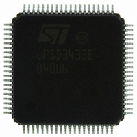
UPSD3433EB40U6 STMicroelectronics, UPSD3433EB40U6 Datasheet - Page 186

UPSD3433EB40U6
Manufacturer Part Number
UPSD3433EB40U6
Description
MCU 8BIT 8032 128KB FLASH 80TQFP
Manufacturer
STMicroelectronics
Series
µPSDr
Datasheet
1.UPSD3434EB40T6.pdf
(293 pages)
Specifications of UPSD3433EB40U6
Core Processor
8032
Core Size
8-Bit
Speed
40MHz
Connectivity
I²C, IrDA, SPI, UART/USART, USB
Peripherals
LVD, POR, PWM, WDT
Number Of I /o
46
Program Memory Size
160KB (160K x 8)
Program Memory Type
FLASH
Ram Size
8K x 8
Voltage - Supply (vcc/vdd)
3 V ~ 5.5 V
Data Converters
A/D 8x10b
Oscillator Type
Internal
Operating Temperature
-40°C ~ 85°C
Package / Case
80-TQFP, 80-VQFP
For Use With
497-5518 - EVAL BOARD RFID READER497-5046 - KIT TOOL FOR ST7/UPSD/STR7 MCU
Lead Free Status / RoHS Status
Lead free / RoHS Compliant
Eeprom Size
-
Other names
497-5660
Available stocks
Company
Part Number
Manufacturer
Quantity
Price
Company:
Part Number:
UPSD3433EB40U6
Manufacturer:
STMicroelectronics
Quantity:
10 000
- Current page: 186 of 293
- Download datasheet (5Mb)
PSD module
28.1.1
28.1.2
28.1.3
28.1.4
186/293
8032 address/data/control interface
These signals attach directly to the MCU Module to implement a 16-bit multiplexed 8051-
style bus between the two stacked die. The MCU instruction prefetch and branch cache
logic resides on the MCU Module, leaving a modified 8051-style memory interface on the
PSD Module.
The active-low reset signal originating from the MCU Module goes to the PSD Module reset
input (RST). This reset signal can then be routed as an external output from the uPSD34xx
to the system PC board, if needed, through any one of the PLD output pins as active-high or
active-low logic by specifying logic equations in PSDsoft Express.
The 8032 address and data busses are routed throughout the PSD Module as shown in
Figure 62
not only connected to the memories, but also to the General PLD, making it possible for the
8032 to directly read and write individual logic macrocells inside the General PLD.
Dual Flash memories and IAP
uPSD34xx devices contain two independent Flash memory arrays. This means that the
8032 can read instructions from one Flash memory array while erasing or writing the other
Flash memory array. Concurrent operation like this enables robust remote updates of
firmware, also known as In-Application Programming (IAP). IAP can occur using any
uPSD34xx interface (e.g., UART, I2C, SPI). Concurrent memory operation also enables the
designer to emulate EEPROM memory within either of the two Flash memory arrays for
small data sets that have frequent updates.
The 8032 can erase Flash memories by individual sectors or it can erase an entire Flash
memory array at one time. Each sector in either Flash memory may be individually write
protected, blocking any WRITEs from the 8032 (good for boot and start-up code protection).
The Flash memories automatically go to standby between 8032 READ or WRITE accesses
to conserve power. Minimum erase cycles is 100K and minimum data retention is 15 years.
Flash memory, as well as the entire PSD Module may be programmed with the JTAG In-
System Programming (ISP) interface with no 8032 involvement, good for manufacturing and
lab development.
Main Flash memory
The Main Flash memory is divided into equal sized sectors that are individually selectable
by the Decode PLD output signals, named FSx, one signal for each Main Flash memory
sector. Each Flash sector can be located at any address within 8032 program address
space (accessed with PSEN) or data address space, also known as 8032 XDATA space
(accessed with RD or WR), as defined with the software development tool, PSDsoft
Express. The user only has to specify an address range for each segment and specify if
Main Flash memory will reside in 8032 data or program address space, and then PSEN, RD,
or WR are automatically activated for the specified range. 8032 firmware is easily
programmed into Main Flash memory using PSDsoft Express or other software tools. See
Table 101 on page 187
Secondary Flash memory
The smaller Secondary Flash memory is also divided into equal sized sectors that are
individually selectable by the Decode PLD signals, named CSBOOTx, one signal for each
Secondary Flash memory sector. Each sector can be located at any address within 8032
connecting many elements on the PSD Module to the 8032 MCU. The 8032 bus is
for Main Flash sector sizes on the various uPSD34xx devices.
uPSD34xx
Related parts for UPSD3433EB40U6
Image
Part Number
Description
Manufacturer
Datasheet
Request
R

Part Number:
Description:
MCU 8BIT 8032 128KB FLASH 80TQFP
Manufacturer:
STMicroelectronics
Datasheet:

Part Number:
Description:
MCU 8BIT 8032 128KB FLASH 52TQFP
Manufacturer:
STMicroelectronics
Datasheet:

Part Number:
Description:
STMicroelectronics [RIPPLE-CARRY BINARY COUNTER/DIVIDERS]
Manufacturer:
STMicroelectronics
Datasheet:

Part Number:
Description:
STMicroelectronics [LIQUID-CRYSTAL DISPLAY DRIVERS]
Manufacturer:
STMicroelectronics
Datasheet:

Part Number:
Description:
BOARD EVAL FOR MEMS SENSORS
Manufacturer:
STMicroelectronics
Datasheet:

Part Number:
Description:
NPN TRANSISTOR POWER MODULE
Manufacturer:
STMicroelectronics
Datasheet:

Part Number:
Description:
TURBOSWITCH ULTRA-FAST HIGH VOLTAGE DIODE
Manufacturer:
STMicroelectronics
Datasheet:

Part Number:
Description:
Manufacturer:
STMicroelectronics
Datasheet:

Part Number:
Description:
DIODE / SCR MODULE
Manufacturer:
STMicroelectronics
Datasheet:

Part Number:
Description:
DIODE / SCR MODULE
Manufacturer:
STMicroelectronics
Datasheet:

Part Number:
Description:
Search -----> STE16N100
Manufacturer:
STMicroelectronics
Datasheet:

Part Number:
Description:
Search ---> STE53NA50
Manufacturer:
STMicroelectronics
Datasheet:


