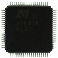
UPSD3433EB40U6 STMicroelectronics, UPSD3433EB40U6 Datasheet - Page 112

UPSD3433EB40U6
Manufacturer Part Number
UPSD3433EB40U6
Description
MCU 8BIT 8032 128KB FLASH 80TQFP
Manufacturer
STMicroelectronics
Series
µPSDr
Datasheet
1.UPSD3434EB40T6.pdf
(293 pages)
Specifications of UPSD3433EB40U6
Core Processor
8032
Core Size
8-Bit
Speed
40MHz
Connectivity
I²C, IrDA, SPI, UART/USART, USB
Peripherals
LVD, POR, PWM, WDT
Number Of I /o
46
Program Memory Size
160KB (160K x 8)
Program Memory Type
FLASH
Ram Size
8K x 8
Voltage - Supply (vcc/vdd)
3 V ~ 5.5 V
Data Converters
A/D 8x10b
Oscillator Type
Internal
Operating Temperature
-40°C ~ 85°C
Package / Case
80-TQFP, 80-VQFP
For Use With
497-5518 - EVAL BOARD RFID READER497-5046 - KIT TOOL FOR ST7/UPSD/STR7 MCU
Lead Free Status / RoHS Status
Lead free / RoHS Compliant
Eeprom Size
-
Other names
497-5660
Available stocks
Company
Part Number
Manufacturer
Quantity
Price
Company:
Part Number:
UPSD3433EB40U6
Manufacturer:
STMicroelectronics
Quantity:
10 000
- Current page: 112 of 293
- Download datasheet (5Mb)
IrDA interface
22.1
112/293
The UART1 serial channel can operate in one of four different modes as shown in
on page 100
used for IrDA communication, UART1 must operate in Mode 1 only, to be compatible with
IrDA protocol up to 115.2k bps. The IrDA interface will support baud rates generated from
Timer 1 or Timer 2, just like standard UART serial communication, but with one restriction.
The transmit baud rate and receive baud rate must be the same (cannot be different rates as
is allowed by standard UART communications).
The IrDA Interface is disabled after a reset and is enabled by setting the IRDAEN Bit in the
SFR named IRDACON
and TxD signals will bypass the internal IrDA logic and instead they are routed directly to the
pins RxD1 and TxD1 respectively. When IrDA is enabled, the IrDA pulse shaping logic is
active and resides between UART1 and the pins RxD1 and TxD1 as shown in
page
Baud rate selection
The IrDA standard only supports 2.4, 9.6, 19.2, and 115.2kbps.
informs the IrDA Interface of the baud rate of UART#1 so that it can perform pulse
modulation properly. It may not be necessary to implement the BR[3:0] bits in the IRDACON
Register if the IrDA Interface obtains the proper timing from UART#1.
Table 50.
Bit 7
4-0
Bit
–
7
6
5
111.
CDIV[4:0]
IRDACON register bit definition (SFR CEh, reset value 0Fh)
in
IRDAEN
IRDAEN
Symbol
PULSE
Bit 6
Section 21: Serial UART interfaces on page
–
(Table 50 on page
PULSE
Bit 5
R/W
RW
RW
RW
–
Reserved
IrDA Enable
0 = IrDA Interface is disabled
1 = IrDA is enabled, UART1 outputs are disconnected from
Port 1 (or Port 4)
IrDA Pulse Modulation Select
0 = 1.627µs
1 = 3/16 bit time pulses
Specify Clock Divider (see
CDIV4
Bit 4
112). When IrDA is disabled, the UART1's RxD
CDIV3
Bit 3
Definition
Table 53 on page
99. However, when UART1 is
CDIV2
Bit 2
Table 52 on page 113
CDIV1
Bit 1
114)
Figure 39 on
uPSD34xx
Table 46
CDIV0
Bit 0
Related parts for UPSD3433EB40U6
Image
Part Number
Description
Manufacturer
Datasheet
Request
R

Part Number:
Description:
MCU 8BIT 8032 128KB FLASH 80TQFP
Manufacturer:
STMicroelectronics
Datasheet:

Part Number:
Description:
MCU 8BIT 8032 128KB FLASH 52TQFP
Manufacturer:
STMicroelectronics
Datasheet:

Part Number:
Description:
STMicroelectronics [RIPPLE-CARRY BINARY COUNTER/DIVIDERS]
Manufacturer:
STMicroelectronics
Datasheet:

Part Number:
Description:
STMicroelectronics [LIQUID-CRYSTAL DISPLAY DRIVERS]
Manufacturer:
STMicroelectronics
Datasheet:

Part Number:
Description:
BOARD EVAL FOR MEMS SENSORS
Manufacturer:
STMicroelectronics
Datasheet:

Part Number:
Description:
NPN TRANSISTOR POWER MODULE
Manufacturer:
STMicroelectronics
Datasheet:

Part Number:
Description:
TURBOSWITCH ULTRA-FAST HIGH VOLTAGE DIODE
Manufacturer:
STMicroelectronics
Datasheet:

Part Number:
Description:
Manufacturer:
STMicroelectronics
Datasheet:

Part Number:
Description:
DIODE / SCR MODULE
Manufacturer:
STMicroelectronics
Datasheet:

Part Number:
Description:
DIODE / SCR MODULE
Manufacturer:
STMicroelectronics
Datasheet:

Part Number:
Description:
Search -----> STE16N100
Manufacturer:
STMicroelectronics
Datasheet:

Part Number:
Description:
Search ---> STE53NA50
Manufacturer:
STMicroelectronics
Datasheet:


