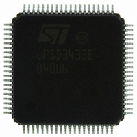
UPSD3433EB40U6 STMicroelectronics, UPSD3433EB40U6 Datasheet - Page 188

UPSD3433EB40U6
Manufacturer Part Number
UPSD3433EB40U6
Description
MCU 8BIT 8032 128KB FLASH 80TQFP
Manufacturer
STMicroelectronics
Series
µPSDr
Datasheet
1.UPSD3434EB40T6.pdf
(293 pages)
Specifications of UPSD3433EB40U6
Core Processor
8032
Core Size
8-Bit
Speed
40MHz
Connectivity
I²C, IrDA, SPI, UART/USART, USB
Peripherals
LVD, POR, PWM, WDT
Number Of I /o
46
Program Memory Size
160KB (160K x 8)
Program Memory Type
FLASH
Ram Size
8K x 8
Voltage - Supply (vcc/vdd)
3 V ~ 5.5 V
Data Converters
A/D 8x10b
Oscillator Type
Internal
Operating Temperature
-40°C ~ 85°C
Package / Case
80-TQFP, 80-VQFP
For Use With
497-5518 - EVAL BOARD RFID READER497-5046 - KIT TOOL FOR ST7/UPSD/STR7 MCU
Lead Free Status / RoHS Status
Lead free / RoHS Compliant
Eeprom Size
-
Other names
497-5660
Available stocks
Company
Part Number
Manufacturer
Quantity
Price
Company:
Part Number:
UPSD3433EB40U6
Manufacturer:
STMicroelectronics
Quantity:
10 000
- Current page: 188 of 293
- Download datasheet (5Mb)
PSD module
28.1.8
28.1.9
28.1.10
188/293
signals used to “page” memory beyond the 64K byte limit (program space or XDATA). Most
8051 compilers directly support memory paging, also known as memory banking. If memory
paging is not needed, or if not all eight page register bits are needed for memory paging, the
remaining bits may be used in the General PLD for general logic. Page Register outputs are
cleared to logic ’0’ at reset and power-up.
Programmable logic (PLDs)
The uPSD34xx contains two PLDs
or Non-Turbo mode. PLDs operate faster (less propagation delay) while in Turbo mode but
consume more power than in Non-Turbo mode. Non-Turbo mode allows the PLDs to go to
standby automatically when no PLD inputs are changing to conserve power.
The logic configuration (from equations) of both PLDs is stored with non-volatile Flash
technology and the logic is active upon power-up. PLDs may NOT be programmed by the
8032, PLD programming only occurs through the JTAG interface.
Figure 63. Memory page register
PLD #1, decode PLD (DPLD)
This programmable logic implements memory mapping and is used to select one of the
individual Main Flash memory segments, one of individual Secondary Flash memory
segments, the SRAM, or the group of csiop registers when the 8032 presents an address to
DPLD inputs (see
select signals on Port D pins. The DPLD also optionally produces two select signals (PSEL0
and PSEL1) used to enable a special data bus repeater function on Port A, referred to as
Peripheral I/O Mode. There are 69 DPLD input signals which include: 8032 address and
control signals, Page Register outputs, PSD Module Port pin inputs, and GPLD logic
feedback.
PLD #2, general PLD (GPLD)
This programmable logic is used to create both combinatorial and sequential general
purpose logic (see
(OMCs) and 20 Input Macrocells (IMCs). Output Macrocell registers are unique in that they
have direct connection to the 8032 data bus allowing them to be loaded and read directly by
the 8032 at runtime through OMC registers in csiop. This direct access is good for making
Figure 75 on page
Figure 76 on page
RST
(PSD Module Reset)
offset E0h
Read via
Load or
csiop +
8032
Data
Bus
D0
D1
D2
D3
D4
D5
D6
D7
Register
Page
(Figure 74 on page
RST
217). The DPLD can also optionally drive external chip
218). The GPLD contains 16 Output Macrocells
Q0
Q1
Q2
Q3
Q4
Q5
Q6
Q7
PGR0-7
DPLD
GPLD
and
215) that may optionally run in Turbo
General
Selects
Chip-
Logic
and
AI09172
uPSD34xx
Related parts for UPSD3433EB40U6
Image
Part Number
Description
Manufacturer
Datasheet
Request
R

Part Number:
Description:
MCU 8BIT 8032 128KB FLASH 80TQFP
Manufacturer:
STMicroelectronics
Datasheet:

Part Number:
Description:
MCU 8BIT 8032 128KB FLASH 52TQFP
Manufacturer:
STMicroelectronics
Datasheet:

Part Number:
Description:
STMicroelectronics [RIPPLE-CARRY BINARY COUNTER/DIVIDERS]
Manufacturer:
STMicroelectronics
Datasheet:

Part Number:
Description:
STMicroelectronics [LIQUID-CRYSTAL DISPLAY DRIVERS]
Manufacturer:
STMicroelectronics
Datasheet:

Part Number:
Description:
BOARD EVAL FOR MEMS SENSORS
Manufacturer:
STMicroelectronics
Datasheet:

Part Number:
Description:
NPN TRANSISTOR POWER MODULE
Manufacturer:
STMicroelectronics
Datasheet:

Part Number:
Description:
TURBOSWITCH ULTRA-FAST HIGH VOLTAGE DIODE
Manufacturer:
STMicroelectronics
Datasheet:

Part Number:
Description:
Manufacturer:
STMicroelectronics
Datasheet:

Part Number:
Description:
DIODE / SCR MODULE
Manufacturer:
STMicroelectronics
Datasheet:

Part Number:
Description:
DIODE / SCR MODULE
Manufacturer:
STMicroelectronics
Datasheet:

Part Number:
Description:
Search -----> STE16N100
Manufacturer:
STMicroelectronics
Datasheet:

Part Number:
Description:
Search ---> STE53NA50
Manufacturer:
STMicroelectronics
Datasheet:


