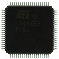
UPSD3433EB40U6 STMicroelectronics, UPSD3433EB40U6 Datasheet - Page 199

UPSD3433EB40U6
Manufacturer Part Number
UPSD3433EB40U6
Description
MCU 8BIT 8032 128KB FLASH 80TQFP
Manufacturer
STMicroelectronics
Series
µPSDr
Datasheet
1.UPSD3434EB40T6.pdf
(293 pages)
Specifications of UPSD3433EB40U6
Core Processor
8032
Core Size
8-Bit
Speed
40MHz
Connectivity
I²C, IrDA, SPI, UART/USART, USB
Peripherals
LVD, POR, PWM, WDT
Number Of I /o
46
Program Memory Size
160KB (160K x 8)
Program Memory Type
FLASH
Ram Size
8K x 8
Voltage - Supply (vcc/vdd)
3 V ~ 5.5 V
Data Converters
A/D 8x10b
Oscillator Type
Internal
Operating Temperature
-40°C ~ 85°C
Package / Case
80-TQFP, 80-VQFP
For Use With
497-5518 - EVAL BOARD RFID READER497-5046 - KIT TOOL FOR ST7/UPSD/STR7 MCU
Lead Free Status / RoHS Status
Lead free / RoHS Compliant
Eeprom Size
-
Other names
497-5660
Available stocks
Company
Part Number
Manufacturer
Quantity
Price
Company:
Part Number:
UPSD3433EB40U6
Manufacturer:
STMicroelectronics
Quantity:
10 000
- Current page: 199 of 293
- Download datasheet (5Mb)
uPSD34xx
Note:
28.4
The Flash memories are 16-bit wide when it is in Program Memory space and are 8-bit wide
when it is in the Data Space. When the Flash memory is configured in both “Program
Space” and “Data Space,” the Flash will drive 16-bit in a PSEN cycle and operates as an 8-
bit memory in READ or WRITE cycle.
The SRAM, csiop, and external device are always in 8-bit data space.
Table 105. Data width in different bus cycles
x = NA
Runtime control register definitions (csiop)
The 39 csiop registers are defined in
address offset (specified in
in PSDsoft Express. Do not write to unused locations within the csiop block of 256 registers,
they should remain logic zero.
Table 106. CSIOP registers and their offsets (in hexadecimal)
PSEN Cycle (Program Memory)
Read or Write Cycle (Data Memory)
Flash Programming Cycle (Flash Write
or Reading Status)
Data In
Control
Data Out
Direction
Register
Name
Type of Bus Cycle
(80-pin)
Port A
00h
02h
04h
06h
Port B Port C Port D Other
01h
03h
05h
07h
Table
10h
12h
14h
106) added to the csiop base address that was specified
Table
Main Flash
11h
13h
15h
16-bit
8-bit
8-bit
106. The 8032 can access each register by the
Secondary
MCU I/O input mode. Read to
obtain current logic level of pins
on Ports A, B, C, or D. No
WRITEs.
Selects MCUI/O or Latched
Address Out mode. Logic 0 =
MCU I/O, 1 = 8032 Addr Out.
Write to select mode. Read for
status.
MCU I/O output mode. Write to
set logic level on pins of Ports
A, B, C, or D. Read to check
status. This register has no
effect if a port pin is driven by
an OMC output from PLD.
MCU I/O mode. Configures
port pin as input or output.
Write to set direction of port
pins.
Logic 1 = out, Logic 0 = in.
Read to check status.
Flash
16-bit
8-bit
8-bit
Description
SRAM
8-bit
x
x
CSIOP
8-bit
x
x
PSD module
Table 122
Table 134
Table 126
Table 130
page 228
page 232
page 229
page 229
External
Device
8-bit
Link
199/293
on
on
on
on
x
x
Related parts for UPSD3433EB40U6
Image
Part Number
Description
Manufacturer
Datasheet
Request
R

Part Number:
Description:
MCU 8BIT 8032 128KB FLASH 80TQFP
Manufacturer:
STMicroelectronics
Datasheet:

Part Number:
Description:
MCU 8BIT 8032 128KB FLASH 52TQFP
Manufacturer:
STMicroelectronics
Datasheet:

Part Number:
Description:
STMicroelectronics [RIPPLE-CARRY BINARY COUNTER/DIVIDERS]
Manufacturer:
STMicroelectronics
Datasheet:

Part Number:
Description:
STMicroelectronics [LIQUID-CRYSTAL DISPLAY DRIVERS]
Manufacturer:
STMicroelectronics
Datasheet:

Part Number:
Description:
BOARD EVAL FOR MEMS SENSORS
Manufacturer:
STMicroelectronics
Datasheet:

Part Number:
Description:
NPN TRANSISTOR POWER MODULE
Manufacturer:
STMicroelectronics
Datasheet:

Part Number:
Description:
TURBOSWITCH ULTRA-FAST HIGH VOLTAGE DIODE
Manufacturer:
STMicroelectronics
Datasheet:

Part Number:
Description:
Manufacturer:
STMicroelectronics
Datasheet:

Part Number:
Description:
DIODE / SCR MODULE
Manufacturer:
STMicroelectronics
Datasheet:

Part Number:
Description:
DIODE / SCR MODULE
Manufacturer:
STMicroelectronics
Datasheet:

Part Number:
Description:
Search -----> STE16N100
Manufacturer:
STMicroelectronics
Datasheet:

Part Number:
Description:
Search ---> STE53NA50
Manufacturer:
STMicroelectronics
Datasheet:


