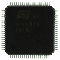
UPSD3433EB40U6 STMicroelectronics, UPSD3433EB40U6 Datasheet - Page 119

UPSD3433EB40U6
Manufacturer Part Number
UPSD3433EB40U6
Description
MCU 8BIT 8032 128KB FLASH 80TQFP
Manufacturer
STMicroelectronics
Series
µPSDr
Datasheet
1.UPSD3434EB40T6.pdf
(293 pages)
Specifications of UPSD3433EB40U6
Core Processor
8032
Core Size
8-Bit
Speed
40MHz
Connectivity
I²C, IrDA, SPI, UART/USART, USB
Peripherals
LVD, POR, PWM, WDT
Number Of I /o
46
Program Memory Size
160KB (160K x 8)
Program Memory Type
FLASH
Ram Size
8K x 8
Voltage - Supply (vcc/vdd)
3 V ~ 5.5 V
Data Converters
A/D 8x10b
Oscillator Type
Internal
Operating Temperature
-40°C ~ 85°C
Package / Case
80-TQFP, 80-VQFP
For Use With
497-5518 - EVAL BOARD RFID READER497-5046 - KIT TOOL FOR ST7/UPSD/STR7 MCU
Lead Free Status / RoHS Status
Lead free / RoHS Compliant
Eeprom Size
-
Other names
497-5660
Available stocks
Company
Part Number
Manufacturer
Quantity
Price
Company:
Part Number:
UPSD3433EB40U6
Manufacturer:
STMicroelectronics
Quantity:
10 000
- Current page: 119 of 293
- Download datasheet (5Mb)
uPSD34xx
23.6
23.7
General call address
A General Call (GC) occurs when a Master-Transmitter initiates a transfer containing a
Slave address of 0000000b, and the R/W bit is logic 0. All Slave devices capable of
responding to this broadcast message will acknowledge the GC simultaneously and then
behave as a Slave-Receiver. The next byte transmitted by the Master will be accepted and
acknowledged by all Slaves capable of handling the special data bytes. A Slave that cannot
handle one of these data bytes must ignore it by not acknowledging it. The I
lists the possible meanings of the special bytes that follow the first GC address byte, and the
actions to be taken by the Slave device(s) upon receiving them. A common use of the GC by
a Master is to dynamically assign device addresses to Slave devices on the bus capable of a
programmable device address.
The uPSD34xx can generate a GC as a Master-Transmitter, and it can receive a GC as a
Slave. When receiving a GC address (00h), an interrupt will be generated so firmware may
respond to the special GC data bytes if desired.
Serial I/O engine (SIOE)
At the heart of the I
automatically handles low-level I
clock generation and synchronization) and it is controlled and monitored by five SFRs.
The five SFRs shown in
●
●
●
●
●
S1CON - Interface Control
S1STA - Interface Status
S1DAT - Data Shift Register
S1ADR - Device Address
S1SETUP - Sampling Rate
2
C interface is the hardware SIOE, shown in
Figure 43
(Table 56 on page
(Table 58 on page
(Table 54 on page
2
(Table 59 on page
C bus protocol (data shifting, handshaking, arbitration,
(Table 57 on page
are:
123)
124)
121)
125)
124)
Figure
43. The SIOE
2
C specification
I
2
C interface
119/293
Related parts for UPSD3433EB40U6
Image
Part Number
Description
Manufacturer
Datasheet
Request
R

Part Number:
Description:
MCU 8BIT 8032 128KB FLASH 80TQFP
Manufacturer:
STMicroelectronics
Datasheet:

Part Number:
Description:
MCU 8BIT 8032 128KB FLASH 52TQFP
Manufacturer:
STMicroelectronics
Datasheet:

Part Number:
Description:
STMicroelectronics [RIPPLE-CARRY BINARY COUNTER/DIVIDERS]
Manufacturer:
STMicroelectronics
Datasheet:

Part Number:
Description:
STMicroelectronics [LIQUID-CRYSTAL DISPLAY DRIVERS]
Manufacturer:
STMicroelectronics
Datasheet:

Part Number:
Description:
BOARD EVAL FOR MEMS SENSORS
Manufacturer:
STMicroelectronics
Datasheet:

Part Number:
Description:
NPN TRANSISTOR POWER MODULE
Manufacturer:
STMicroelectronics
Datasheet:

Part Number:
Description:
TURBOSWITCH ULTRA-FAST HIGH VOLTAGE DIODE
Manufacturer:
STMicroelectronics
Datasheet:

Part Number:
Description:
Manufacturer:
STMicroelectronics
Datasheet:

Part Number:
Description:
DIODE / SCR MODULE
Manufacturer:
STMicroelectronics
Datasheet:

Part Number:
Description:
DIODE / SCR MODULE
Manufacturer:
STMicroelectronics
Datasheet:

Part Number:
Description:
Search -----> STE16N100
Manufacturer:
STMicroelectronics
Datasheet:

Part Number:
Description:
Search ---> STE53NA50
Manufacturer:
STMicroelectronics
Datasheet:


