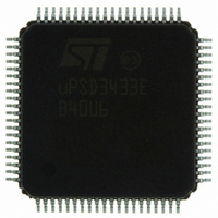
UPSD3433EB40U6 STMicroelectronics, UPSD3433EB40U6 Datasheet - Page 80

UPSD3433EB40U6
Manufacturer Part Number
UPSD3433EB40U6
Description
MCU 8BIT 8032 128KB FLASH 80TQFP
Manufacturer
STMicroelectronics
Series
µPSDr
Datasheet
1.UPSD3434EB40T6.pdf
(293 pages)
Specifications of UPSD3433EB40U6
Core Processor
8032
Core Size
8-Bit
Speed
40MHz
Connectivity
I²C, IrDA, SPI, UART/USART, USB
Peripherals
LVD, POR, PWM, WDT
Number Of I /o
46
Program Memory Size
160KB (160K x 8)
Program Memory Type
FLASH
Ram Size
8K x 8
Voltage - Supply (vcc/vdd)
3 V ~ 5.5 V
Data Converters
A/D 8x10b
Oscillator Type
Internal
Operating Temperature
-40°C ~ 85°C
Package / Case
80-TQFP, 80-VQFP
For Use With
497-5518 - EVAL BOARD RFID READER497-5046 - KIT TOOL FOR ST7/UPSD/STR7 MCU
Lead Free Status / RoHS Status
Lead free / RoHS Compliant
Eeprom Size
-
Other names
497-5660
Available stocks
Company
Part Number
Manufacturer
Quantity
Price
Company:
Part Number:
UPSD3433EB40U6
Manufacturer:
STMicroelectronics
Quantity:
10 000
- Current page: 80 of 293
- Download datasheet (5Mb)
MCU bus interface
18.5
Note:
80/293
1
2
3
It is not possible to specify in the BUSCON Register a different number of MCU_CLK
periods for various address ranges. For example, the user cannot specify 4 MCU_CLK
periods for RD read cycles to one address range on the PSD Module, and 5 MCU_CLK
periods for RD read cycles to a different address range on an external device. However, the
user can specify one number of clock periods for PSEN read cycles and a different number
of clock periods for RD or WR cycles (see
Controlling the PFQ and BC
The BUSCON Register allows firmware to enable and disable the PFQ and BC at run-time.
Sometimes it may be desired to disable the PFQ and BC to ensure deterministic execution.
The dynamic action of the PFQ and BC may cause varying program execution times
depending on the events that happen prior to a particular section of code of interest. For this
reason, it is not recommended to implement timing loops in firmware, but instead use one of
the many hardware timers in the uPSD34xx. By default, the PFQ and BC are enabled after a
reset condition.
Important note: Disabling the PFQ or BC will seriously reduce MCU performance.
Figure 22. A RD or PSEN bus cycle set to 5 MCU_CLK
The PSEN cycle is 16-bit, while the RD cycle is 8-bit only.
A PSEN bus cycle in progress may be aborted before completion if the PFQ and Branch
Cache (BC) determines the current code fetch cycle is not needed.
Whenever the same number of MCU_CLK periods is specified in BUSCON for both PSEN
and RD cycles, the bus cycle timing is typically identical for each of these types of bus
cycles. In this case, the only time PSEN read cycles are longer than RD read cycles is when
the PFQ issues a stall while reloading. PFQ stalls do not affect RD read cycles. By
comparison, in many traditional 8051 architectures, RD bus cycles are always longer than
PSEN bus cycles.
RD/PSEN
MCU Clock
AD0-AD15
(2,3)
ALE
1
A0-A15
2
Figure 22 on page
5-Clock Bus Cycle
3
80).
4
D0-D15 (1)
5
AI10436
uPSD34xx
Related parts for UPSD3433EB40U6
Image
Part Number
Description
Manufacturer
Datasheet
Request
R

Part Number:
Description:
MCU 8BIT 8032 128KB FLASH 80TQFP
Manufacturer:
STMicroelectronics
Datasheet:

Part Number:
Description:
MCU 8BIT 8032 128KB FLASH 52TQFP
Manufacturer:
STMicroelectronics
Datasheet:

Part Number:
Description:
STMicroelectronics [RIPPLE-CARRY BINARY COUNTER/DIVIDERS]
Manufacturer:
STMicroelectronics
Datasheet:

Part Number:
Description:
STMicroelectronics [LIQUID-CRYSTAL DISPLAY DRIVERS]
Manufacturer:
STMicroelectronics
Datasheet:

Part Number:
Description:
BOARD EVAL FOR MEMS SENSORS
Manufacturer:
STMicroelectronics
Datasheet:

Part Number:
Description:
NPN TRANSISTOR POWER MODULE
Manufacturer:
STMicroelectronics
Datasheet:

Part Number:
Description:
TURBOSWITCH ULTRA-FAST HIGH VOLTAGE DIODE
Manufacturer:
STMicroelectronics
Datasheet:

Part Number:
Description:
Manufacturer:
STMicroelectronics
Datasheet:

Part Number:
Description:
DIODE / SCR MODULE
Manufacturer:
STMicroelectronics
Datasheet:

Part Number:
Description:
DIODE / SCR MODULE
Manufacturer:
STMicroelectronics
Datasheet:

Part Number:
Description:
Search -----> STE16N100
Manufacturer:
STMicroelectronics
Datasheet:

Part Number:
Description:
Search ---> STE53NA50
Manufacturer:
STMicroelectronics
Datasheet:


