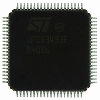
UPSD3433EB40U6 STMicroelectronics, UPSD3433EB40U6 Datasheet - Page 204

UPSD3433EB40U6
Manufacturer Part Number
UPSD3433EB40U6
Description
MCU 8BIT 8032 128KB FLASH 80TQFP
Manufacturer
STMicroelectronics
Series
µPSDr
Datasheet
1.UPSD3434EB40T6.pdf
(293 pages)
Specifications of UPSD3433EB40U6
Core Processor
8032
Core Size
8-Bit
Speed
40MHz
Connectivity
I²C, IrDA, SPI, UART/USART, USB
Peripherals
LVD, POR, PWM, WDT
Number Of I /o
46
Program Memory Size
160KB (160K x 8)
Program Memory Type
FLASH
Ram Size
8K x 8
Voltage - Supply (vcc/vdd)
3 V ~ 5.5 V
Data Converters
A/D 8x10b
Oscillator Type
Internal
Operating Temperature
-40°C ~ 85°C
Package / Case
80-TQFP, 80-VQFP
For Use With
497-5518 - EVAL BOARD RFID READER497-5046 - KIT TOOL FOR ST7/UPSD/STR7 MCU
Lead Free Status / RoHS Status
Lead free / RoHS Compliant
Eeprom Size
-
Other names
497-5660
Available stocks
Company
Part Number
Manufacturer
Quantity
Price
Company:
Part Number:
UPSD3433EB40U6
Manufacturer:
STMicroelectronics
Quantity:
10 000
- Current page: 204 of 293
- Download datasheet (5Mb)
PSD module
28.5.3
28.5.4
28.5.5
28.5.6
204/293
3
sequences. The individual sector select signal (FS0 - FS7 or CSBOOT0-CSBOOT3) which
is active during the instruction sequence determines the complete address.
Directing this command to any individual sector within a Flash memory array will invoke the
bulk erase of all Flash memory sectors within that array.
Reading Flash memory
Under typical conditions, the 8032 may read the Flash memory using READ operations
(READ bus cycles) just as it would a ROM or RAM device. Alternately, the 8032 may use
READ operations to obtain status information about a Program or Erase operation that is
currently in progress. The following sections describe the kinds of READ operations.
Read memory contents.
Flash memory is placed in the Read Array mode after Power-up, after a PSD Module reset
event, or after receiving a Reset Flash memory instruction sequence from the 8032. The
8032 can read Flash memory contents using standard READ bus cycles anytime the Flash
array is in Read Array mode. Flash memories will always be in Read Array mode when the
array is not actively engaged in a program or erase operation.
Reading the erase/program status bits
The Flash arrays provide several status bits to be used by the 8032 to confirm the
completion of an erase or program operation on Flash memory, shown in
page
complete.
The 8032 performs a READ operation to obtain these status bits while an erase or program
operation is being executed by the state machine inside each Flash memory array.
Data polling flag (DQ7)
While programming either Flash memory, the 8032 may read the Data Polling Flag Bit
(DQ7), which outputs the complement of the D7 Bit of the byte being programmed into Flash
memory. Once the program operation is complete, DQ7 is equal to D7 of the byte just
programmed into Flash memory, indicating the program cycle has completed successfully.
The correct select signal, FSx or CSBOOTx, must be active during the entire polling
procedure.
Polling may also be used to indicate when an erase operation has completed. During an
erase operation, DQ7 is '0.' After the erase is complete DQ7 is '1.' The correct select signal,
FSx or CSBOOTx, must be active during the entire polling procedure.
DQ7 is valid after the fourth instruction byte WRITE operation (for program instruction
sequence) or after the sixth instruction byte WRITE operation (for erase instruction
sequence).
If all Flash memory sectors to be erased are protected, DQ7 is reset to ’0’ for about 100µs,
and then DQ7 returns to the value of D7 of the previously addressed byte. No erasure is
performed.
206. The status bits can be read as many times as needed until an operation is
Table 108 on
uPSD34xx
Related parts for UPSD3433EB40U6
Image
Part Number
Description
Manufacturer
Datasheet
Request
R

Part Number:
Description:
MCU 8BIT 8032 128KB FLASH 80TQFP
Manufacturer:
STMicroelectronics
Datasheet:

Part Number:
Description:
MCU 8BIT 8032 128KB FLASH 52TQFP
Manufacturer:
STMicroelectronics
Datasheet:

Part Number:
Description:
STMicroelectronics [RIPPLE-CARRY BINARY COUNTER/DIVIDERS]
Manufacturer:
STMicroelectronics
Datasheet:

Part Number:
Description:
STMicroelectronics [LIQUID-CRYSTAL DISPLAY DRIVERS]
Manufacturer:
STMicroelectronics
Datasheet:

Part Number:
Description:
BOARD EVAL FOR MEMS SENSORS
Manufacturer:
STMicroelectronics
Datasheet:

Part Number:
Description:
NPN TRANSISTOR POWER MODULE
Manufacturer:
STMicroelectronics
Datasheet:

Part Number:
Description:
TURBOSWITCH ULTRA-FAST HIGH VOLTAGE DIODE
Manufacturer:
STMicroelectronics
Datasheet:

Part Number:
Description:
Manufacturer:
STMicroelectronics
Datasheet:

Part Number:
Description:
DIODE / SCR MODULE
Manufacturer:
STMicroelectronics
Datasheet:

Part Number:
Description:
DIODE / SCR MODULE
Manufacturer:
STMicroelectronics
Datasheet:

Part Number:
Description:
Search -----> STE16N100
Manufacturer:
STMicroelectronics
Datasheet:

Part Number:
Description:
Search ---> STE53NA50
Manufacturer:
STMicroelectronics
Datasheet:


