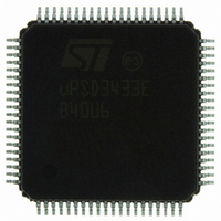
UPSD3433EB40U6 STMicroelectronics, UPSD3433EB40U6 Datasheet - Page 168

UPSD3433EB40U6
Manufacturer Part Number
UPSD3433EB40U6
Description
MCU 8BIT 8032 128KB FLASH 80TQFP
Manufacturer
STMicroelectronics
Series
µPSDr
Datasheet
1.UPSD3434EB40T6.pdf
(293 pages)
Specifications of UPSD3433EB40U6
Core Processor
8032
Core Size
8-Bit
Speed
40MHz
Connectivity
I²C, IrDA, SPI, UART/USART, USB
Peripherals
LVD, POR, PWM, WDT
Number Of I /o
46
Program Memory Size
160KB (160K x 8)
Program Memory Type
FLASH
Ram Size
8K x 8
Voltage - Supply (vcc/vdd)
3 V ~ 5.5 V
Data Converters
A/D 8x10b
Oscillator Type
Internal
Operating Temperature
-40°C ~ 85°C
Package / Case
80-TQFP, 80-VQFP
For Use With
497-5518 - EVAL BOARD RFID READER497-5046 - KIT TOOL FOR ST7/UPSD/STR7 MCU
Lead Free Status / RoHS Status
Lead free / RoHS Compliant
Eeprom Size
-
Other names
497-5660
Available stocks
Company
Part Number
Manufacturer
Quantity
Price
Company:
Part Number:
UPSD3433EB40U6
Manufacturer:
STMicroelectronics
Quantity:
10 000
- Current page: 168 of 293
- Download datasheet (5Mb)
USB interface
168/293
●
Table 85.
Table 86.
Bit 7
7:6
5:0
Bit
BASEADDR[7:6]
Bit 7
USB FIFO Base Address High and Low Registers (UBASEH and UBASEL)
All 10 Endpoint FIFOs share the same 64-byte address range. The 16-bit base
address for the FIFOs is specified using the USB Base Address registers (see
and
the direction and the Endpoint for the FIFO that is accessed when addressing the 64-
bytes of XDATA space starting with the base address specified in the Base Address
Registers. The Base Address is a 64-byte segment where the lower 6 bits of the base
register are hardwired to '0.'
Important note: The USB FIFO Base Address must be set to an open 64-byte segment
in the XDATA space. Care should be taken to ensure that there is no overlap of
addresses between the USB FIFOs and the flash memory, SRAM, csiop registers, and
anything else accessed in the XDATA space. While the logic in the PSD module
handles overlap of flash memory, SRAM, and the csiop registers with a fixed priority
(see
case with the USB FIFOs. Unpredictable results as well as potential damage to the
device may occur if there is an overlap of addresses.
7:0
Bit
Table
Section 28.1: PSD module functional description on page
BASEADDR
BASEADDR
Symbol
USB FIFO base address high register (UBASEH 0F3h, reset value 00h)
USB FIFO base address low register (UBASEL 0F4h, reset value 00h)
BASEADDR
[7:6]
[5:0]
Bit 6
Symbol
86). The USB Endpoint Select Register (see
[15:8]
Bit 6
R/W
R/W
Bit 5
R
0
Bit 5
R/W
R/W
Bits 7 and 6 of the 16-bit base address for the USB FIFOs to
be mapped in XDATA space
Hardwired '0'
BASEADDR[15:8]
Bit 4
The upper 8 bits of the 16-bit base address for USB FIFOs
to be mapped in XDATA space
0
Bit 4
Bit 3
0
Bit 3
Definition
Definition
Bit 2
Table 82 on page
Bit 2
0
185), this is not the
Bit 1
Bit 1
0
165) selects
uPSD34xx
Table 85
Bit 0
Bit 0
0
Related parts for UPSD3433EB40U6
Image
Part Number
Description
Manufacturer
Datasheet
Request
R

Part Number:
Description:
MCU 8BIT 8032 128KB FLASH 80TQFP
Manufacturer:
STMicroelectronics
Datasheet:

Part Number:
Description:
MCU 8BIT 8032 128KB FLASH 52TQFP
Manufacturer:
STMicroelectronics
Datasheet:

Part Number:
Description:
STMicroelectronics [RIPPLE-CARRY BINARY COUNTER/DIVIDERS]
Manufacturer:
STMicroelectronics
Datasheet:

Part Number:
Description:
STMicroelectronics [LIQUID-CRYSTAL DISPLAY DRIVERS]
Manufacturer:
STMicroelectronics
Datasheet:

Part Number:
Description:
BOARD EVAL FOR MEMS SENSORS
Manufacturer:
STMicroelectronics
Datasheet:

Part Number:
Description:
NPN TRANSISTOR POWER MODULE
Manufacturer:
STMicroelectronics
Datasheet:

Part Number:
Description:
TURBOSWITCH ULTRA-FAST HIGH VOLTAGE DIODE
Manufacturer:
STMicroelectronics
Datasheet:

Part Number:
Description:
Manufacturer:
STMicroelectronics
Datasheet:

Part Number:
Description:
DIODE / SCR MODULE
Manufacturer:
STMicroelectronics
Datasheet:

Part Number:
Description:
DIODE / SCR MODULE
Manufacturer:
STMicroelectronics
Datasheet:

Part Number:
Description:
Search -----> STE16N100
Manufacturer:
STMicroelectronics
Datasheet:

Part Number:
Description:
Search ---> STE53NA50
Manufacturer:
STMicroelectronics
Datasheet:


