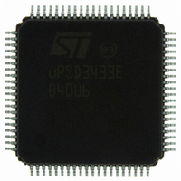
UPSD3433EB40U6 STMicroelectronics, UPSD3433EB40U6 Datasheet - Page 143

UPSD3433EB40U6
Manufacturer Part Number
UPSD3433EB40U6
Description
MCU 8BIT 8032 128KB FLASH 80TQFP
Manufacturer
STMicroelectronics
Series
µPSDr
Datasheet
1.UPSD3434EB40T6.pdf
(293 pages)
Specifications of UPSD3433EB40U6
Core Processor
8032
Core Size
8-Bit
Speed
40MHz
Connectivity
I²C, IrDA, SPI, UART/USART, USB
Peripherals
LVD, POR, PWM, WDT
Number Of I /o
46
Program Memory Size
160KB (160K x 8)
Program Memory Type
FLASH
Ram Size
8K x 8
Voltage - Supply (vcc/vdd)
3 V ~ 5.5 V
Data Converters
A/D 8x10b
Oscillator Type
Internal
Operating Temperature
-40°C ~ 85°C
Package / Case
80-TQFP, 80-VQFP
For Use With
497-5518 - EVAL BOARD RFID READER497-5046 - KIT TOOL FOR ST7/UPSD/STR7 MCU
Lead Free Status / RoHS Status
Lead free / RoHS Compliant
Eeprom Size
-
Other names
497-5660
Available stocks
Company
Part Number
Manufacturer
Quantity
Price
Company:
Part Number:
UPSD3433EB40U6
Manufacturer:
STMicroelectronics
Quantity:
10 000
- Current page: 143 of 293
- Download datasheet (5Mb)
uPSD34xx
25
Note:
1
2
USB interface
uPSD34xx devices provide a full speed USB (Universal Serial Bus) device interface. The
serial interface engine (SIE) provides the interface between the CPU and the USB (see
Figure
For a list of known limitations of USB interface for uPSD34xx devices, please refer to
Section 34: Important notes on page
Please make sure you have the latest 3400 USB firmware.
The USB module supports the following features:
●
●
●
●
●
●
●
●
●
●
The analog front-end of the USB module is an on-chip USB transceiver. It is designed to
allow voltage levels equal to V
of the USB. It is capable of receiving and transmitting serial data at full speed (12 Mb/s).
The SIE is the digital-front-end of the USB block. This module recovers the 12MHz clock,
detects the USB sync word, and handles all low-level USB protocols and error checking.
The bit-clock recovery circuit recovers the clock from the incoming USB data stream and is
able to track jitter and frequency drift according to the USB specifications.
The SIE also translates the electrical USB signals into bytes or signals. When there is a
USB device address match, the USB data is directed to an endpoint’s FIFO for OUT
transactions and read from an endpoint’s FIFO for IN transactions. Control transfers are
supported on Endpoint0 and interrupt and bulk data transfers are supported on Endpoints1
through 4. The device’s USB address and the enabling of the endpoints are programmable
using the SIE’s SFRs.
Important note: The USB SIE requires a 48MHz clock to operate properly. A PLL is included
in the uPSD34xx that must be programmed appropriately based on the input clock to
provide a 48MHz clock to the SIE (see
PLL).
USB 2.0 compliant to full-speed mode (12 Mbps)
3.3V USB transceiver
Five endpoints including Control endpoint 0
–
–
USB Bus Suspend detection and Resume generation
PLL Multiplier to generate the 48 MHz as required for USB support.
Interrupts for various USB bus conditions.
Performs NRZI encoding and decoding, bit stuffing, CRC generation and checking, and
serial/parallel data conversion
Double buffering (using FIFO pairing) for efficient data transfer in Bulk transfer
Busy bit-based FIFO status monitoring
FIFOs accessible via XDATA space
49).
Each endpoint includes two 64 byte FIFOs, one for IN and one for OUT
transactions
Endpoints 1 through 4 support Interrupt and Bulk transfers
DD
from the standard logic to interface with the physical layer
287.
Section 14.2.2: USB_CLK on page 60
USB interface
to set up the
143/293
Related parts for UPSD3433EB40U6
Image
Part Number
Description
Manufacturer
Datasheet
Request
R

Part Number:
Description:
MCU 8BIT 8032 128KB FLASH 80TQFP
Manufacturer:
STMicroelectronics
Datasheet:

Part Number:
Description:
MCU 8BIT 8032 128KB FLASH 52TQFP
Manufacturer:
STMicroelectronics
Datasheet:

Part Number:
Description:
STMicroelectronics [RIPPLE-CARRY BINARY COUNTER/DIVIDERS]
Manufacturer:
STMicroelectronics
Datasheet:

Part Number:
Description:
STMicroelectronics [LIQUID-CRYSTAL DISPLAY DRIVERS]
Manufacturer:
STMicroelectronics
Datasheet:

Part Number:
Description:
BOARD EVAL FOR MEMS SENSORS
Manufacturer:
STMicroelectronics
Datasheet:

Part Number:
Description:
NPN TRANSISTOR POWER MODULE
Manufacturer:
STMicroelectronics
Datasheet:

Part Number:
Description:
TURBOSWITCH ULTRA-FAST HIGH VOLTAGE DIODE
Manufacturer:
STMicroelectronics
Datasheet:

Part Number:
Description:
Manufacturer:
STMicroelectronics
Datasheet:

Part Number:
Description:
DIODE / SCR MODULE
Manufacturer:
STMicroelectronics
Datasheet:

Part Number:
Description:
DIODE / SCR MODULE
Manufacturer:
STMicroelectronics
Datasheet:

Part Number:
Description:
Search -----> STE16N100
Manufacturer:
STMicroelectronics
Datasheet:

Part Number:
Description:
Search ---> STE53NA50
Manufacturer:
STMicroelectronics
Datasheet:


