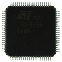
UPSD3433EB40U6 STMicroelectronics, UPSD3433EB40U6 Datasheet - Page 192

UPSD3433EB40U6
Manufacturer Part Number
UPSD3433EB40U6
Description
MCU 8BIT 8032 128KB FLASH 80TQFP
Manufacturer
STMicroelectronics
Series
µPSDr
Datasheet
1.UPSD3434EB40T6.pdf
(293 pages)
Specifications of UPSD3433EB40U6
Core Processor
8032
Core Size
8-Bit
Speed
40MHz
Connectivity
I²C, IrDA, SPI, UART/USART, USB
Peripherals
LVD, POR, PWM, WDT
Number Of I /o
46
Program Memory Size
160KB (160K x 8)
Program Memory Type
FLASH
Ram Size
8K x 8
Voltage - Supply (vcc/vdd)
3 V ~ 5.5 V
Data Converters
A/D 8x10b
Oscillator Type
Internal
Operating Temperature
-40°C ~ 85°C
Package / Case
80-TQFP, 80-VQFP
For Use With
497-5518 - EVAL BOARD RFID READER497-5046 - KIT TOOL FOR ST7/UPSD/STR7 MCU
Lead Free Status / RoHS Status
Lead free / RoHS Compliant
Eeprom Size
-
Other names
497-5660
Available stocks
Company
Part Number
Manufacturer
Quantity
Price
Company:
Part Number:
UPSD3433EB40U6
Manufacturer:
STMicroelectronics
Quantity:
10 000
- Current page: 192 of 293
- Download datasheet (5Mb)
PSD module
28.2.1
28.2.2
28.2.3
192/293
8032 program address space
In the example of
three memory pages in the upper half of program address space, and the remaining two
sectors of Main Flash memory (fs0, fs1) reside in the lower half of program address space,
and these two sectors are independent of paging (they reside in “common” program address
space). This paged memory example is quite common and supported by many 8051
software compilers.
8032 data address space (XDATA)
Four sectors of Secondary Flash memory reside in the upper half of 8032 XDATA space in
the example of
The 8032 SFR registers and local SRAM inside the 8032 MCU Module do not reside in
XDATA space, so it is OK to place PSD Module SRAM or csiop registers at an address that
overlaps the address of internal 8032 MCU Module SRAM and registers.
Figure 64. Typical system memory map
Specifying the memory map with PSDsoft express
The memory map example shown in
Express in a point-and-click environment. PSDsoft Express will automatically generate
Hardware Definition Language (HDL) statements of the ABEL language for the DPLD, such
as those shown in
Specifying these equations using PSDsoft Express is very simple. For example,
page 84 shows how to specify the chip-select equation for the 16K byte Flash memory
segment, fs4. Notice fs4 is on memory page 1. This specification process is repeated for all
other Flash memory segments, the SRAM, the csiop register block, and any external chip
select signals that may be needed.
Figure
FFFFh
C000h
8000h
4000h
0000h
Figure
Table
64. SRAM and csiop registers are in the lower half of XDATA space.
Common Memory to All Pages
Common Memory to All Pages
Page 0
103.
64, six sectors of Main Flash memory (fs2.. fs7) are paged across
16KB
16KB
fs3
fs2
8032 PROGRAM SPACE
fs1, 16KB
fs0, 16KB
Page 1
(PSEN)
16KB
16KB
fs5
fs4
Figure 64 on page 192
Page 2
16KB
16KB
fs7
fs6
(RD and WR)
8032 XDATA
rs0, 8KB
csboot3
csboot0
csboot2
csboot1
System
SPACE
Page X
csiop
256B
8KB
8KB
8KB
8KB
I/O
AI09173
is implemented using PSDsoft
FFFFh
E000h
C000h
A000h
8000h
2000h
0000h
Figure
uPSD34xx
65,
Related parts for UPSD3433EB40U6
Image
Part Number
Description
Manufacturer
Datasheet
Request
R

Part Number:
Description:
MCU 8BIT 8032 128KB FLASH 80TQFP
Manufacturer:
STMicroelectronics
Datasheet:

Part Number:
Description:
MCU 8BIT 8032 128KB FLASH 52TQFP
Manufacturer:
STMicroelectronics
Datasheet:

Part Number:
Description:
STMicroelectronics [RIPPLE-CARRY BINARY COUNTER/DIVIDERS]
Manufacturer:
STMicroelectronics
Datasheet:

Part Number:
Description:
STMicroelectronics [LIQUID-CRYSTAL DISPLAY DRIVERS]
Manufacturer:
STMicroelectronics
Datasheet:

Part Number:
Description:
BOARD EVAL FOR MEMS SENSORS
Manufacturer:
STMicroelectronics
Datasheet:

Part Number:
Description:
NPN TRANSISTOR POWER MODULE
Manufacturer:
STMicroelectronics
Datasheet:

Part Number:
Description:
TURBOSWITCH ULTRA-FAST HIGH VOLTAGE DIODE
Manufacturer:
STMicroelectronics
Datasheet:

Part Number:
Description:
Manufacturer:
STMicroelectronics
Datasheet:

Part Number:
Description:
DIODE / SCR MODULE
Manufacturer:
STMicroelectronics
Datasheet:

Part Number:
Description:
DIODE / SCR MODULE
Manufacturer:
STMicroelectronics
Datasheet:

Part Number:
Description:
Search -----> STE16N100
Manufacturer:
STMicroelectronics
Datasheet:

Part Number:
Description:
Search ---> STE53NA50
Manufacturer:
STMicroelectronics
Datasheet:


