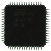
UPSD3433EB40U6 STMicroelectronics, UPSD3433EB40U6 Datasheet - Page 234

UPSD3433EB40U6
Manufacturer Part Number
UPSD3433EB40U6
Description
MCU 8BIT 8032 128KB FLASH 80TQFP
Manufacturer
STMicroelectronics
Series
µPSDr
Datasheet
1.UPSD3434EB40T6.pdf
(293 pages)
Specifications of UPSD3433EB40U6
Core Processor
8032
Core Size
8-Bit
Speed
40MHz
Connectivity
I²C, IrDA, SPI, UART/USART, USB
Peripherals
LVD, POR, PWM, WDT
Number Of I /o
46
Program Memory Size
160KB (160K x 8)
Program Memory Type
FLASH
Ram Size
8K x 8
Voltage - Supply (vcc/vdd)
3 V ~ 5.5 V
Data Converters
A/D 8x10b
Oscillator Type
Internal
Operating Temperature
-40°C ~ 85°C
Package / Case
80-TQFP, 80-VQFP
For Use With
497-5518 - EVAL BOARD RFID READER497-5046 - KIT TOOL FOR ST7/UPSD/STR7 MCU
Lead Free Status / RoHS Status
Lead free / RoHS Compliant
Eeprom Size
-
Other names
497-5660
Available stocks
Company
Part Number
Manufacturer
Quantity
Price
Company:
Part Number:
UPSD3433EB40U6
Manufacturer:
STMicroelectronics
Quantity:
10 000
- Current page: 234 of 293
- Download datasheet (5Mb)
PSD module
28.5.41
28.5.42
28.5.43
Note:
28.5.44
Note:
28.5.45
234/293
JTAG ISP mode
Four of the pins on Port C are based on the IEEE 1149.1 JTAG specification and are used
for In-System Programming (ISP) of the PSD Module and debugging of the 8032 MCU
Module. These pins (TDI, TDO, TMS, TCK) are dedicated to JTAG and cannot be used for
any other I/O function. There are two optional pins on Port C (TSTAT and TERR) that can be
used to reduce programming time during ISP. See
debug on page
Other port capabilities
It is possible to change the type of output drive on the ports at run-time. It is also possible to
read the state of the output enable signal of the output driver at run-time. The following
sections provide the details.
Port pin drive options
The csiop Drive Select registers allow reconfiguration of the output drive type for certain
pins on Ports A, B, C, and D. The 8032 can change the default drive type setting at run-time.
The is no action needed in PSDsoft Express to change or define these pin output drive
types.
pin output driver. The default setting for drive type for all pins on Ports A, B, C, and D is a
standard CMOS push-pull output driver.
When a pin on Port A, B, C, D is not used as an output and has no external device driving it
as an input (floating pin), excess power consumption can be avoided by placing a weak pull-
up resistor (100K
Drive select registers
The csiop Drive Select Registers will configure a pin output driver as Open Drain or CMOS
push/pull for some port pins, and controls the slew rate for other port pins. An external pull-
up resistor should be used for pins configured as Open Drain, and the resistor should be
sized not to exceed the current sink capability of the pin (see DC specifications). Open Drain
outputs are diode clamped, thus the maximum voltage on an pin configured as Open Drain
is V
A pin can be configured as Open Drain if its corresponding bit in the Drive Select Register is
set to logic '1.'
The slew rate is a measurement of the rise and fall times of an output. A higher slew rate
means a faster output response and may create more electrical noise. A pin operates in a
high slew rate when the corresponding bit in the Drive Register is set to '1.' The default rate
is standard slew rate (see AC specifications).
Table 136
and D. The tables summarize which pins can be configured as Open Drain outputs and
which pins the slew rate can be changed. The default output type is CMOS push/pull output
with normal slew rate.
Enable out registers
The state of the output enable signal for the output driver at each pin on Ports A, B, C, and D
can be read at any time by the 8032 when it reads the csiop Enable Output registers. Logic
'1' means the driver is in output mode, logic ’0’ means the output driver is in high-impedance
DD
Figure 80 on page 226
+ 0.7V.
through
251.
Ω
Table 139 on page 235
) to V
DD
which keeps the CMOS input pin from floating.
shows the csiop Drive Select register output controlling the
show the csiop Drive Registers for Ports A, B, C,
Section 28.6.1: JTAG ISP and JTAG
uPSD34xx
Related parts for UPSD3433EB40U6
Image
Part Number
Description
Manufacturer
Datasheet
Request
R

Part Number:
Description:
MCU 8BIT 8032 128KB FLASH 80TQFP
Manufacturer:
STMicroelectronics
Datasheet:

Part Number:
Description:
MCU 8BIT 8032 128KB FLASH 52TQFP
Manufacturer:
STMicroelectronics
Datasheet:

Part Number:
Description:
STMicroelectronics [RIPPLE-CARRY BINARY COUNTER/DIVIDERS]
Manufacturer:
STMicroelectronics
Datasheet:

Part Number:
Description:
STMicroelectronics [LIQUID-CRYSTAL DISPLAY DRIVERS]
Manufacturer:
STMicroelectronics
Datasheet:

Part Number:
Description:
BOARD EVAL FOR MEMS SENSORS
Manufacturer:
STMicroelectronics
Datasheet:

Part Number:
Description:
NPN TRANSISTOR POWER MODULE
Manufacturer:
STMicroelectronics
Datasheet:

Part Number:
Description:
TURBOSWITCH ULTRA-FAST HIGH VOLTAGE DIODE
Manufacturer:
STMicroelectronics
Datasheet:

Part Number:
Description:
Manufacturer:
STMicroelectronics
Datasheet:

Part Number:
Description:
DIODE / SCR MODULE
Manufacturer:
STMicroelectronics
Datasheet:

Part Number:
Description:
DIODE / SCR MODULE
Manufacturer:
STMicroelectronics
Datasheet:

Part Number:
Description:
Search -----> STE16N100
Manufacturer:
STMicroelectronics
Datasheet:

Part Number:
Description:
Search ---> STE53NA50
Manufacturer:
STMicroelectronics
Datasheet:


