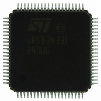
UPSD3433EB40U6 STMicroelectronics, UPSD3433EB40U6 Datasheet - Page 87

UPSD3433EB40U6
Manufacturer Part Number
UPSD3433EB40U6
Description
MCU 8BIT 8032 128KB FLASH 80TQFP
Manufacturer
STMicroelectronics
Series
µPSDr
Datasheet
1.UPSD3434EB40T6.pdf
(293 pages)
Specifications of UPSD3433EB40U6
Core Processor
8032
Core Size
8-Bit
Speed
40MHz
Connectivity
I²C, IrDA, SPI, UART/USART, USB
Peripherals
LVD, POR, PWM, WDT
Number Of I /o
46
Program Memory Size
160KB (160K x 8)
Program Memory Type
FLASH
Ram Size
8K x 8
Voltage - Supply (vcc/vdd)
3 V ~ 5.5 V
Data Converters
A/D 8x10b
Oscillator Type
Internal
Operating Temperature
-40°C ~ 85°C
Package / Case
80-TQFP, 80-VQFP
For Use With
497-5518 - EVAL BOARD RFID READER497-5046 - KIT TOOL FOR ST7/UPSD/STR7 MCU
Lead Free Status / RoHS Status
Lead free / RoHS Compliant
Eeprom Size
-
Other names
497-5660
Available stocks
Company
Part Number
Manufacturer
Quantity
Price
Company:
Part Number:
UPSD3433EB40U6
Manufacturer:
STMicroelectronics
Quantity:
10 000
- Current page: 87 of 293
- Download datasheet (5Mb)
uPSD34xx
20
20.1
20.2
Standard 8032 timer/counters
There are three 8032-style 16-bit Timer/Counter registers (Timer 0, Timer 1, Timer 2) that
can be configured to operate as timers or event counters.
There are two additional 16-bit Timer/Counters in the Programmable Counter Array (PCA),
see
Standard timer SFRs
Timer 0 and Timer 1 have very similar functions, and they share two SFRs for control:
●
●
Timer 0 has two SFRs that form the 16-bit counter, or that can hold reload values, or that
can scale the clock depending on the timer/counter mode:
●
●
Timer 1 has two similar SFRs:
●
●
Timer 2 has one control SFR:
●
Timer 2 has two SFRs that form the 16-bit counter, and perform other functions:
●
●
Timer 2 has two SFRs for capture and reload:
●
●
Clock sources
When enabled in the “Timer” function, the Registers THx and TLx are incremented every
1/12 of the oscillator frequency (f
dividers in the CCON0, stalls from PFQ/BC, or bus transfer cycles. Timers are always
clocked at 1/12 of f
When enabled in the “Counter” function, the Registers THx and TLx are incremented in
response to a 1-to-0 transition sampled at their corresponding external input pin: pin C0 for
Timer 0; pin C1 for Timer 1; or pin T2 for Timer 2. In this function, the external clock input pin
is sampled by the counter at a rate of 1/12 of f
sample, and a logic '0' in the next sample period, the count is incremented at the very next
sample period (period1: sample=1, period2: sample=0, period3: increment count while
continuing to sample). This means the maximum count rate is 1/24 of the f
restrictions on the duty cycle of the external input signal, but to ensure that a given level is
sampled at least once before it changes, it should be active for at least one full sample
Section 27.1: PCA block on page 175
TCON
TMOD
TH0 is the high byte, address 8Ch
TL0 is the low byte, address 8Ah
TH1 is the high byte, address 8Dh
TL1 is the low byte, address 8Bh
T2CON
TH2 is the high byte, address CDh
TL2 is the low byte, address CCh
RCAP2H is the high byte, address CBh
RCAP2L is the low byte, address CAh
(Table 41 on page
(Table 42 on page
(Table 43 on page
OSC
.
88)
90).
93)
OSC
). This timer clock source is not effected by MCU clock
for details.
OSC
. When a logic '1' is determined in one
Standard 8032 timer/counters
OSC
. There are no
87/293
Related parts for UPSD3433EB40U6
Image
Part Number
Description
Manufacturer
Datasheet
Request
R

Part Number:
Description:
MCU 8BIT 8032 128KB FLASH 80TQFP
Manufacturer:
STMicroelectronics
Datasheet:

Part Number:
Description:
MCU 8BIT 8032 128KB FLASH 52TQFP
Manufacturer:
STMicroelectronics
Datasheet:

Part Number:
Description:
STMicroelectronics [RIPPLE-CARRY BINARY COUNTER/DIVIDERS]
Manufacturer:
STMicroelectronics
Datasheet:

Part Number:
Description:
STMicroelectronics [LIQUID-CRYSTAL DISPLAY DRIVERS]
Manufacturer:
STMicroelectronics
Datasheet:

Part Number:
Description:
BOARD EVAL FOR MEMS SENSORS
Manufacturer:
STMicroelectronics
Datasheet:

Part Number:
Description:
NPN TRANSISTOR POWER MODULE
Manufacturer:
STMicroelectronics
Datasheet:

Part Number:
Description:
TURBOSWITCH ULTRA-FAST HIGH VOLTAGE DIODE
Manufacturer:
STMicroelectronics
Datasheet:

Part Number:
Description:
Manufacturer:
STMicroelectronics
Datasheet:

Part Number:
Description:
DIODE / SCR MODULE
Manufacturer:
STMicroelectronics
Datasheet:

Part Number:
Description:
DIODE / SCR MODULE
Manufacturer:
STMicroelectronics
Datasheet:

Part Number:
Description:
Search -----> STE16N100
Manufacturer:
STMicroelectronics
Datasheet:

Part Number:
Description:
Search ---> STE53NA50
Manufacturer:
STMicroelectronics
Datasheet:


