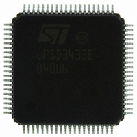
UPSD3433EB40U6 STMicroelectronics, UPSD3433EB40U6 Datasheet - Page 89

UPSD3433EB40U6
Manufacturer Part Number
UPSD3433EB40U6
Description
MCU 8BIT 8032 128KB FLASH 80TQFP
Manufacturer
STMicroelectronics
Series
µPSDr
Datasheet
1.UPSD3434EB40T6.pdf
(293 pages)
Specifications of UPSD3433EB40U6
Core Processor
8032
Core Size
8-Bit
Speed
40MHz
Connectivity
I²C, IrDA, SPI, UART/USART, USB
Peripherals
LVD, POR, PWM, WDT
Number Of I /o
46
Program Memory Size
160KB (160K x 8)
Program Memory Type
FLASH
Ram Size
8K x 8
Voltage - Supply (vcc/vdd)
3 V ~ 5.5 V
Data Converters
A/D 8x10b
Oscillator Type
Internal
Operating Temperature
-40°C ~ 85°C
Package / Case
80-TQFP, 80-VQFP
For Use With
497-5518 - EVAL BOARD RFID READER497-5046 - KIT TOOL FOR ST7/UPSD/STR7 MCU
Lead Free Status / RoHS Status
Lead free / RoHS Compliant
Eeprom Size
-
Other names
497-5660
Available stocks
Company
Part Number
Manufacturer
Quantity
Price
Company:
Part Number:
UPSD3433EB40U6
Manufacturer:
STMicroelectronics
Quantity:
10 000
- Current page: 89 of 293
- Download datasheet (5Mb)
uPSD34xx
20.4
20.5
20.5.1
20.5.2
20.5.3
20.5.4
SFR, TMOD
Timer 0 and Timer 1 have four modes of operation controlled by the SFR named TMOD
(Table
Timer 0 and Timer 1 operating modes
The “Timer” or “Counter” function is selected by the C/T control bits in TMOD. The four
operating modes are selected by bit-pairs M[1:0] in TMOD. Modes 0, 1, and 2 are the same
for both Timer/Counters. Mode 3 is different.
Mode 0
Putting either Timer/Counter into Mode 0 makes it an 8-bit Counter with a divide-by-32 pre-
scaler.
In this mode, the Timer Register is configured as a 13-bit register. As the count rolls over
from all '1s' to all '0s,' it sets the Timer Interrupt flag TF1. The counted input is enabled to the
Timer when TR1 = 1 and either GATE = 0 or EXTINT1 = 1. (Setting GATE = 1 allows the
Timer to be controlled by external input pin, EXTINT1, to facilitate pulse width
measurements). TR1 is a control bit in the SFR, TCON. GATE is a bit in the SFR, TMOD.
The 13-bit register consists of all 8 bits of TH1 and the lower 5 bits of TL1. The upper 3 bits
of TL1 are indeterminate and should be ignored. Setting the run flag, TR1, does not clear
the registers.
Mode 0 operation is the same for the Timer 0 as for Timer 1. Substitute TR0, TF0, C0, TL0,
TH0, and EXTINT0 for the corresponding Timer 1 signals in
different GATE Bits, one for Timer 1 and one for Timer 0.
Mode 1
Mode 1 is the same as Mode 0, except that the Timer Register is being run with all 16 bits.
Mode 2
Mode 2 configures the Timer Register as an 8-bit Counter (TL1) with automatic reload, as
shown in
with the contents of TH1, which is preset with firmware. The reload leaves TH1 unchanged.
Mode 2 operation is the same for Timer/Counter 0.
Mode 3
Timer 1 in Mode 3 simply holds its count. The effect is the same as setting TR1 = 0.
Timer 0 in Mode 3 establishes TL0 and TH0 as two separate counters. The logic for Mode 3
on Timer 0 is shown in
TR0, and TF0, as well as the pin EXTINT0. TH0 is locked into a timer function (counting at a
rate of 1/12 f
controls the “Timer 1“ interrupt flag.
Mode 3 is provided for applications requiring an extra 8-bit timer on the counter (see
Figure 27 on page
three Timer/Counters (not including the PCA). When Timer 0 is in Mode 3, Timer 1 can be
42).
Figure 25
Figure 26 on page
OSC
) and takes over the use of TR1 and TF1 from Timer 1. Thus, TH0 now
shows Mode 0 operation as it applies to Timer 1 (same applies to Timer 0).
91). With Timer 0 in Mode 3, a uPSD34xx device can look like it has
Figure 27 on page
91. Overflow from TL1 not only sets TF1, but also reloads TL1
91. TL0 uses the Timer 0 control Bits: C/T, GATE,
Standard 8032 timer/counters
Figure
25. There are two
89/293
Related parts for UPSD3433EB40U6
Image
Part Number
Description
Manufacturer
Datasheet
Request
R

Part Number:
Description:
MCU 8BIT 8032 128KB FLASH 80TQFP
Manufacturer:
STMicroelectronics
Datasheet:

Part Number:
Description:
MCU 8BIT 8032 128KB FLASH 52TQFP
Manufacturer:
STMicroelectronics
Datasheet:

Part Number:
Description:
STMicroelectronics [RIPPLE-CARRY BINARY COUNTER/DIVIDERS]
Manufacturer:
STMicroelectronics
Datasheet:

Part Number:
Description:
STMicroelectronics [LIQUID-CRYSTAL DISPLAY DRIVERS]
Manufacturer:
STMicroelectronics
Datasheet:

Part Number:
Description:
BOARD EVAL FOR MEMS SENSORS
Manufacturer:
STMicroelectronics
Datasheet:

Part Number:
Description:
NPN TRANSISTOR POWER MODULE
Manufacturer:
STMicroelectronics
Datasheet:

Part Number:
Description:
TURBOSWITCH ULTRA-FAST HIGH VOLTAGE DIODE
Manufacturer:
STMicroelectronics
Datasheet:

Part Number:
Description:
Manufacturer:
STMicroelectronics
Datasheet:

Part Number:
Description:
DIODE / SCR MODULE
Manufacturer:
STMicroelectronics
Datasheet:

Part Number:
Description:
DIODE / SCR MODULE
Manufacturer:
STMicroelectronics
Datasheet:

Part Number:
Description:
Search -----> STE16N100
Manufacturer:
STMicroelectronics
Datasheet:

Part Number:
Description:
Search ---> STE53NA50
Manufacturer:
STMicroelectronics
Datasheet:


