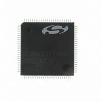
C8051F066-GQ Silicon Laboratories Inc, C8051F066-GQ Datasheet - Page 180

C8051F066-GQ
Manufacturer Part Number
C8051F066-GQ
Description
MCU 8-Bit C8051F06x 8051 CISC 32KB Flash 3.3V 100-Pin TQFP
Manufacturer
Silicon Laboratories Inc
Series
C8051F06xr
Specifications of C8051F066-GQ
Package
100TQFP
Device Core
8051
Family Name
C8051F06x
Maximum Speed
25 MHz
Operating Supply Voltage
3.3 V
Data Bus Width
8 Bit
Number Of Programmable I/os
59
Interface Type
I2C/SMBus/SPI/UART
On-chip Adc
2-chx16-bit
Number Of Timers
5
Ram Size
4.25 KB
Program Memory Size
32 KB
Program Memory Type
Flash
Operating Temperature
-40 to 85 °C
Core Processor
8051
Core Size
8-Bit
Speed
25MHz
Connectivity
EBI/EMI, SMBus (2-Wire/I²C), SPI, UART/USART
Peripherals
Brown-out Detect/Reset, POR, PWM, WDT
Number Of I /o
59
Voltage - Supply (vcc/vdd)
2.7 V ~ 3.6 V
Data Converters
A/D 2x16b
Oscillator Type
Internal
Package / Case
100-TQFP, 100-VQFP
Lead Free Status / RoHS Status
Lead free / RoHS Compliant
Eeprom Size
-
Lead Free Status / RoHS Status
Lead free / RoHS Compliant
Other names
336-1221
Available stocks
Company
Part Number
Manufacturer
Quantity
Price
Company:
Part Number:
C8051F066-GQ
Manufacturer:
Silicon Laboratories Inc
Quantity:
10 000
Company:
Part Number:
C8051F066-GQR
Manufacturer:
Silicon Laboratories Inc
Quantity:
10 000
- Current page: 180 of 328
- Download datasheet (2Mb)
C8051F060/1/2/3/4/5/6/7
180
Flash Read Lock Byte
Bits7-0: Each bit locks a corresponding block of memory. (Bit7 is MSB).
Flash Write/Erase Lock Byte
Bits7-0: Each bit locks a corresponding block of memory.
Flash Access Limit
Read and Write/Erase Security Bits
(Bit 7 is MSB)
Figure 16.1. C8051F060/1/2/3/4/5 Flash Program Memory Map and Security Bytes
Bit
7
6
5
4
3
2
1
0
0: Read operations are locked (disabled) for corresponding block across the JTAG interface.
1: Read operations are unlocked (enabled) for corresponding block across the JTAG inter-
face.
0: Write/Erase operations are locked (disabled) for corresponding block across the JTAG
interface.
1: Write/Erase operations are unlocked (enabled) for corresponding block across the JTAG
interface.
NOTE: When the block containing the security bytes is locked, the security bytes may be
written but not erased.
The Flash Access Limit is defined by the setting of the FLACL register, as described in
Figure 16.3. Firmware running at or above this address is prohibited from using the MOVX
and MOVC instructions to read, write, or erase Flash locations below this address.
0xE000 - 0xFBFD
0xC000 - 0xDFFF
0xA000 - 0xBFFF
Memory Block
0x8000 - 0x9FFF
0x6000 - 0x7FFF
0x4000 - 0x5FFF
0x2000 - 0x3FFF
0x0000 - 0x1FFF
Write/Erase Lock Byte
Read Lock Byte
Memory Space
Program/Data
SFLE = 0
Reserved
Rev. 1.2
0xFFFF
0xFC00
0xFBFF
0xFBFE
0xFBFD
0x0000
Flash Access Limit
Scratchpad Memory
SFLE = 1
(Data only)
0x007F
0x0000
Related parts for C8051F066-GQ
Image
Part Number
Description
Manufacturer
Datasheet
Request
R
Part Number:
Description:
SMD/C°/SINGLE-ENDED OUTPUT SILICON OSCILLATOR
Manufacturer:
Silicon Laboratories Inc
Part Number:
Description:
Manufacturer:
Silicon Laboratories Inc
Datasheet:
Part Number:
Description:
N/A N/A/SI4010 AES KEYFOB DEMO WITH LCD RX
Manufacturer:
Silicon Laboratories Inc
Datasheet:
Part Number:
Description:
N/A N/A/SI4010 SIMPLIFIED KEY FOB DEMO WITH LED RX
Manufacturer:
Silicon Laboratories Inc
Datasheet:
Part Number:
Description:
N/A/-40 TO 85 OC/EZLINK MODULE; F930/4432 HIGH BAND (REV E/B1)
Manufacturer:
Silicon Laboratories Inc
Part Number:
Description:
EZLink Module; F930/4432 Low Band (rev e/B1)
Manufacturer:
Silicon Laboratories Inc
Part Number:
Description:
I°/4460 10 DBM RADIO TEST CARD 434 MHZ
Manufacturer:
Silicon Laboratories Inc
Part Number:
Description:
I°/4461 14 DBM RADIO TEST CARD 868 MHZ
Manufacturer:
Silicon Laboratories Inc
Part Number:
Description:
I°/4463 20 DBM RFSWITCH RADIO TEST CARD 460 MHZ
Manufacturer:
Silicon Laboratories Inc
Part Number:
Description:
I°/4463 20 DBM RADIO TEST CARD 868 MHZ
Manufacturer:
Silicon Laboratories Inc
Part Number:
Description:
I°/4463 27 DBM RADIO TEST CARD 868 MHZ
Manufacturer:
Silicon Laboratories Inc
Part Number:
Description:
I°/4463 SKYWORKS 30 DBM RADIO TEST CARD 915 MHZ
Manufacturer:
Silicon Laboratories Inc
Part Number:
Description:
N/A N/A/-40 TO 85 OC/4463 RFMD 30 DBM RADIO TEST CARD 915 MHZ
Manufacturer:
Silicon Laboratories Inc
Part Number:
Description:
I°/4463 20 DBM RADIO TEST CARD 169 MHZ
Manufacturer:
Silicon Laboratories Inc


