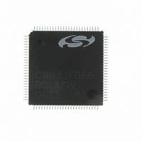
C8051F066-GQ Silicon Laboratories Inc, C8051F066-GQ Datasheet - Page 52

C8051F066-GQ
Manufacturer Part Number
C8051F066-GQ
Description
MCU 8-Bit C8051F06x 8051 CISC 32KB Flash 3.3V 100-Pin TQFP
Manufacturer
Silicon Laboratories Inc
Series
C8051F06xr
Specifications of C8051F066-GQ
Package
100TQFP
Device Core
8051
Family Name
C8051F06x
Maximum Speed
25 MHz
Operating Supply Voltage
3.3 V
Data Bus Width
8 Bit
Number Of Programmable I/os
59
Interface Type
I2C/SMBus/SPI/UART
On-chip Adc
2-chx16-bit
Number Of Timers
5
Ram Size
4.25 KB
Program Memory Size
32 KB
Program Memory Type
Flash
Operating Temperature
-40 to 85 °C
Core Processor
8051
Core Size
8-Bit
Speed
25MHz
Connectivity
EBI/EMI, SMBus (2-Wire/I²C), SPI, UART/USART
Peripherals
Brown-out Detect/Reset, POR, PWM, WDT
Number Of I /o
59
Voltage - Supply (vcc/vdd)
2.7 V ~ 3.6 V
Data Converters
A/D 2x16b
Oscillator Type
Internal
Package / Case
100-TQFP, 100-VQFP
Lead Free Status / RoHS Status
Lead free / RoHS Compliant
Eeprom Size
-
Lead Free Status / RoHS Status
Lead free / RoHS Compliant
Other names
336-1221
Available stocks
Company
Part Number
Manufacturer
Quantity
Price
Company:
Part Number:
C8051F066-GQ
Manufacturer:
Silicon Laboratories Inc
Quantity:
10 000
Company:
Part Number:
C8051F066-GQR
Manufacturer:
Silicon Laboratories Inc
Quantity:
10 000
- Current page: 52 of 328
- Download datasheet (2Mb)
C8051F060/1/2/3/4/5/6/7
5.1.
ADC0 and ADC1 can be programmed to operate independently as single-ended ADCs, or together to
accept a differential input. In single-ended mode, the ADCs can be configured to sample simultaneously, or
to use different conversion speeds. In differential mode, ADC1 is a slave to ADC0, and its configuration is
based on ADC0 settings, except during offset or gain calibrations. The DIFFSEL bit in the Channel Select
Register AMX0SL (Figure 5.6) selects between single-ended and differential mode.
5.1.1. Pseudo-Differential Inputs
The inputs to the ADCs are pseudo-differential. The actual voltage measured by each ADC is equal to the
voltage between the AINn pin and the AINnG pin. AINnG must be a DC signal between -0.2 and 0.6 V. In
most systems, AINnG will be connected to AGND. If not tied to AGND, the AINnG signal can be used to
negate a limited amount of fixed offset, but it is recommended that the internal offset calibration features of
the device be used for this purpose. When operating in differential mode, AIN0G and AIN1G should be tied
together. AINn must remain above AINnG in both modes for accurate conversion results.
52
AIN0G
AIN1G
AIN0
AIN1
Interface
Single-Ended or Differential Operation
DMA
Figure 5.2. 16-bit ADC0 and ADC1 Data Path Diagram
ADC0
ADC1
16-Bit
16-Bit
SAR
SAR
ADC0GTH
ADC1H
16
16
8
16
8
ADC0GTL
ADC1L
Rev. 1.2
+
-
1
0
AMX0SL
Single-Ended
Differential
ADC0LTH
ADC0H
8
16
ADC0LTL
8
ADC0L
Compare
Window
32
AD0WINT
Related parts for C8051F066-GQ
Image
Part Number
Description
Manufacturer
Datasheet
Request
R
Part Number:
Description:
SMD/C°/SINGLE-ENDED OUTPUT SILICON OSCILLATOR
Manufacturer:
Silicon Laboratories Inc
Part Number:
Description:
Manufacturer:
Silicon Laboratories Inc
Datasheet:
Part Number:
Description:
N/A N/A/SI4010 AES KEYFOB DEMO WITH LCD RX
Manufacturer:
Silicon Laboratories Inc
Datasheet:
Part Number:
Description:
N/A N/A/SI4010 SIMPLIFIED KEY FOB DEMO WITH LED RX
Manufacturer:
Silicon Laboratories Inc
Datasheet:
Part Number:
Description:
N/A/-40 TO 85 OC/EZLINK MODULE; F930/4432 HIGH BAND (REV E/B1)
Manufacturer:
Silicon Laboratories Inc
Part Number:
Description:
EZLink Module; F930/4432 Low Band (rev e/B1)
Manufacturer:
Silicon Laboratories Inc
Part Number:
Description:
I°/4460 10 DBM RADIO TEST CARD 434 MHZ
Manufacturer:
Silicon Laboratories Inc
Part Number:
Description:
I°/4461 14 DBM RADIO TEST CARD 868 MHZ
Manufacturer:
Silicon Laboratories Inc
Part Number:
Description:
I°/4463 20 DBM RFSWITCH RADIO TEST CARD 460 MHZ
Manufacturer:
Silicon Laboratories Inc
Part Number:
Description:
I°/4463 20 DBM RADIO TEST CARD 868 MHZ
Manufacturer:
Silicon Laboratories Inc
Part Number:
Description:
I°/4463 27 DBM RADIO TEST CARD 868 MHZ
Manufacturer:
Silicon Laboratories Inc
Part Number:
Description:
I°/4463 SKYWORKS 30 DBM RADIO TEST CARD 915 MHZ
Manufacturer:
Silicon Laboratories Inc
Part Number:
Description:
N/A N/A/-40 TO 85 OC/4463 RFMD 30 DBM RADIO TEST CARD 915 MHZ
Manufacturer:
Silicon Laboratories Inc
Part Number:
Description:
I°/4463 20 DBM RADIO TEST CARD 169 MHZ
Manufacturer:
Silicon Laboratories Inc


