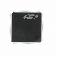
C8051F066-GQ Silicon Laboratories Inc, C8051F066-GQ Datasheet - Page 75

C8051F066-GQ
Manufacturer Part Number
C8051F066-GQ
Description
MCU 8-Bit C8051F06x 8051 CISC 32KB Flash 3.3V 100-Pin TQFP
Manufacturer
Silicon Laboratories Inc
Series
C8051F06xr
Specifications of C8051F066-GQ
Package
100TQFP
Device Core
8051
Family Name
C8051F06x
Maximum Speed
25 MHz
Operating Supply Voltage
3.3 V
Data Bus Width
8 Bit
Number Of Programmable I/os
59
Interface Type
I2C/SMBus/SPI/UART
On-chip Adc
2-chx16-bit
Number Of Timers
5
Ram Size
4.25 KB
Program Memory Size
32 KB
Program Memory Type
Flash
Operating Temperature
-40 to 85 °C
Core Processor
8051
Core Size
8-Bit
Speed
25MHz
Connectivity
EBI/EMI, SMBus (2-Wire/I²C), SPI, UART/USART
Peripherals
Brown-out Detect/Reset, POR, PWM, WDT
Number Of I /o
59
Voltage - Supply (vcc/vdd)
2.7 V ~ 3.6 V
Data Converters
A/D 2x16b
Oscillator Type
Internal
Package / Case
100-TQFP, 100-VQFP
Lead Free Status / RoHS Status
Lead free / RoHS Compliant
Eeprom Size
-
Lead Free Status / RoHS Status
Lead free / RoHS Compliant
Other names
336-1221
Available stocks
Company
Part Number
Manufacturer
Quantity
Price
Company:
Part Number:
C8051F066-GQ
Manufacturer:
Silicon Laboratories Inc
Quantity:
10 000
Company:
Part Number:
C8051F066-GQR
Manufacturer:
Silicon Laboratories Inc
Quantity:
10 000
- Current page: 75 of 328
- Download datasheet (2Mb)
6.
The DMA interface works in conjunction with ADC0 and ADC1 to write ADC outputs directly to a specified
region of XRAM. The DMA interface is configured by software using the Special Function Registers shown
in Figure 6.1. Up to 64 instructions can be programmed into the Instruction Buffer to designate a sequence
of DMA operations. The Instruction Buffer is accessed by the DMA Control Logic, which gathers the appro-
priate data from the ADCs and controls writes to XRAM. The DMA instructions tell the DMA Control Logic
which ADC(s) to expect results from, but do not initiate the actual conversions. It is important to configure
the ADCs for the desired start-of-conversion source, voltage reference, and SAR clock frequency prior to
starting the DMA interface. For information on setting up the ADCs, refer to
and ADC1)” on page
6.1.
The Instruction Buffer has 64 8-bit locations that can be programmed with a sequence of DMA instructions.
Filling the Instruction Buffer is done with the Special Function Registers DMA0IPT (DMA Instruction Write
Address Register, Figure 6.6) and DMA0IDT (DMA Instruction Write Data Register, Figure 6.7). Instruc-
tions are written to the Instruction Buffer at address DMA0IPT when the instruction word is written to
DMA0IDT. Reading the register DMA0IDT will return the instruction word at location DMA0IPT. After a write
or read operation on DMA0IDT, the DMA0IPT register is automatically incremented to the next Instruction
Buffer location.
Direct Memory Access Interface (DMA0)
Writing to the Instruction Buffer
AIN0G
AIN1G
Current Address
Start Address
AIN0
AIN1
DMA0BND
DMA0ISW
DMA0IPT
Address
51.
ADC0
ADC1
Instruction
(64 Bytes)
Write Logic
Buffer
Instruction Data
DMA0IDT
DMA0CTH
Figure 6.1. DMA0 Block Diagram
Repeat Counter Limit
DMA0CTL
Rev. 1.2
DMA0CF
Control Logic
C8051F060/1/2/3/4/5/6/7
DMA
DMA0CSH
DMA0CN
Current Repeat Counter Value
DMA0DSH
DMA0DAH
Address Bus
Data Bus
Section “5. 16-Bit ADCs (ADC0
Beginning XRAM Address
Current XRAM Address
DMA0CSL
(on-chip or
off-chip)
DMA0DSL
DMA0DAL
XRAM
75
Related parts for C8051F066-GQ
Image
Part Number
Description
Manufacturer
Datasheet
Request
R
Part Number:
Description:
SMD/C°/SINGLE-ENDED OUTPUT SILICON OSCILLATOR
Manufacturer:
Silicon Laboratories Inc
Part Number:
Description:
Manufacturer:
Silicon Laboratories Inc
Datasheet:
Part Number:
Description:
N/A N/A/SI4010 AES KEYFOB DEMO WITH LCD RX
Manufacturer:
Silicon Laboratories Inc
Datasheet:
Part Number:
Description:
N/A N/A/SI4010 SIMPLIFIED KEY FOB DEMO WITH LED RX
Manufacturer:
Silicon Laboratories Inc
Datasheet:
Part Number:
Description:
N/A/-40 TO 85 OC/EZLINK MODULE; F930/4432 HIGH BAND (REV E/B1)
Manufacturer:
Silicon Laboratories Inc
Part Number:
Description:
EZLink Module; F930/4432 Low Band (rev e/B1)
Manufacturer:
Silicon Laboratories Inc
Part Number:
Description:
I°/4460 10 DBM RADIO TEST CARD 434 MHZ
Manufacturer:
Silicon Laboratories Inc
Part Number:
Description:
I°/4461 14 DBM RADIO TEST CARD 868 MHZ
Manufacturer:
Silicon Laboratories Inc
Part Number:
Description:
I°/4463 20 DBM RFSWITCH RADIO TEST CARD 460 MHZ
Manufacturer:
Silicon Laboratories Inc
Part Number:
Description:
I°/4463 20 DBM RADIO TEST CARD 868 MHZ
Manufacturer:
Silicon Laboratories Inc
Part Number:
Description:
I°/4463 27 DBM RADIO TEST CARD 868 MHZ
Manufacturer:
Silicon Laboratories Inc
Part Number:
Description:
I°/4463 SKYWORKS 30 DBM RADIO TEST CARD 915 MHZ
Manufacturer:
Silicon Laboratories Inc
Part Number:
Description:
N/A N/A/-40 TO 85 OC/4463 RFMD 30 DBM RADIO TEST CARD 915 MHZ
Manufacturer:
Silicon Laboratories Inc
Part Number:
Description:
I°/4463 20 DBM RADIO TEST CARD 169 MHZ
Manufacturer:
Silicon Laboratories Inc


