C8051F066-GQ Silicon Laboratories Inc, C8051F066-GQ Datasheet - Page 5
C8051F066-GQ
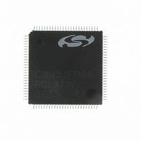
Manufacturer Part Number
C8051F066-GQ
Description
MCU 8-Bit C8051F06x 8051 CISC 32KB Flash 3.3V 100-Pin TQFP
Manufacturer
Silicon Laboratories Inc
Series
C8051F06xr
Specifications of C8051F066-GQ
Package
100TQFP
Device Core
8051
Family Name
C8051F06x
Maximum Speed
25 MHz
Operating Supply Voltage
3.3 V
Data Bus Width
8 Bit
Number Of Programmable I/os
59
Interface Type
I2C/SMBus/SPI/UART
On-chip Adc
2-chx16-bit
Number Of Timers
5
Ram Size
4.25 KB
Program Memory Size
32 KB
Program Memory Type
Flash
Operating Temperature
-40 to 85 °C
Core Processor
8051
Core Size
8-Bit
Speed
25MHz
Connectivity
EBI/EMI, SMBus (2-Wire/I²C), SPI, UART/USART
Peripherals
Brown-out Detect/Reset, POR, PWM, WDT
Number Of I /o
59
Voltage - Supply (vcc/vdd)
2.7 V ~ 3.6 V
Data Converters
A/D 2x16b
Oscillator Type
Internal
Package / Case
100-TQFP, 100-VQFP
Lead Free Status / RoHS Status
Lead free / RoHS Compliant
Eeprom Size
-
Lead Free Status / RoHS Status
Lead free / RoHS Compliant
Other names
336-1221
Available stocks
Company
Part Number
Manufacturer
Quantity
Price
Company:

Part Number:
C8051F066-GQ
Manufacturer:
Silicon Laboratories Inc
Quantity:
10 000
Company:
Part Number:
C8051F066-GQR
Manufacturer:
Silicon Laboratories Inc
Quantity:
10 000


15. Oscillators ............................................................................................................. 171
16. Flash Memory ....................................................................................................... 177
17. External Data Memory Interface and On-Chip XRAM........................................ 187
18. Port Input/Output.................................................................................................. 203
15.1.Programmable Internal Oscillator ................................................................... 171
15.2.External Oscillator Drive Circuit...................................................................... 173
15.3.System Clock Selection.................................................................................. 173
15.4.External Crystal Example ............................................................................... 175
15.5.External RC Example ..................................................................................... 175
15.6.External Capacitor Example ........................................................................... 175
16.1.Programming The Flash Memory ................................................................... 177
16.2.Non-volatile Data Storage .............................................................................. 178
16.3.Security Options ............................................................................................. 179
17.1.Accessing XRAM............................................................................................ 187
17.2.Configuring the External Memory Interface .................................................... 188
17.3.Port Selection and Configuration.................................................................... 188
17.4.Multiplexed and Non-multiplexed Selection.................................................... 190
17.5.Memory Mode Selection................................................................................. 192
17.6.Timing .......................................................................................................... 194
18.1.Ports 0 through 3 and the Priority Crossbar Decoder..................................... 205
14.7.1.Enable/Reset WDT ................................................................................ 166
14.7.2.Disable WDT .......................................................................................... 166
14.7.3.Disable WDT Lockout ............................................................................ 166
14.7.4.Setting WDT Interval .............................................................................. 166
16.3.1.Summary of Flash Security Options....................................................... 183
17.1.1.16-Bit MOVX Example ........................................................................... 187
17.1.2.8-Bit MOVX Example ............................................................................. 187
17.4.1.Multiplexed Configuration....................................................................... 190
17.4.2.Non-multiplexed Configuration............................................................... 191
17.5.1.Internal XRAM Only ............................................................................... 192
17.5.2.Split Mode without Bank Select.............................................................. 192
17.5.3.Split Mode with Bank Select................................................................... 193
17.5.4.External Only.......................................................................................... 193
17.6.1.Non-multiplexed Mode ........................................................................... 196
17.6.2.Multiplexed Mode ................................................................................... 199
18.1.1.Crossbar Pin Assignment and Allocation ............................................... 205
18.1.2.Configuring the Output Modes of the Port Pins...................................... 206
18.1.3.Configuring Port Pins as Digital Inputs................................................... 207
18.1.4.Weak Pull-ups ........................................................................................ 207
17.6.1.1.16-bit MOVX: EMI0CF[4:2] = ‘101’, ‘110’, or ‘111’......................... 196
17.6.1.2.8-bit MOVX without Bank Select: EMI0CF[4:2] = ‘101’ or ‘111’..... 197
17.6.1.3.8-bit MOVX with Bank Select: EMI0CF[4:2] = ‘110’....................... 198
17.6.2.1.16-bit MOVX: EMI0CF[4:2] = ‘001’, ‘010’, or ‘011’......................... 199
17.6.2.2.8-bit MOVX without Bank Select: EMI0CF[4:2] = ‘001’ or ‘011’..... 200
17.6.2.3.8-bit MOVX with Bank Select: EMI0CF[4:2] = ‘010’....................... 201
Rev. 1.2
C8051F060/1/2/3/4/5/6/7
5
Related parts for C8051F066-GQ
Image
Part Number
Description
Manufacturer
Datasheet
Request
R

Part Number:
Description:
SMD/C°/SINGLE-ENDED OUTPUT SILICON OSCILLATOR
Manufacturer:
Silicon Laboratories Inc
Part Number:
Description:
Manufacturer:
Silicon Laboratories Inc
Datasheet:
Part Number:
Description:
N/A N/A/SI4010 AES KEYFOB DEMO WITH LCD RX
Manufacturer:
Silicon Laboratories Inc
Datasheet:
Part Number:
Description:
N/A N/A/SI4010 SIMPLIFIED KEY FOB DEMO WITH LED RX
Manufacturer:
Silicon Laboratories Inc
Datasheet:
Part Number:
Description:
N/A/-40 TO 85 OC/EZLINK MODULE; F930/4432 HIGH BAND (REV E/B1)
Manufacturer:
Silicon Laboratories Inc
Part Number:
Description:
EZLink Module; F930/4432 Low Band (rev e/B1)
Manufacturer:
Silicon Laboratories Inc
Part Number:
Description:
I°/4460 10 DBM RADIO TEST CARD 434 MHZ
Manufacturer:
Silicon Laboratories Inc
Part Number:
Description:
I°/4461 14 DBM RADIO TEST CARD 868 MHZ
Manufacturer:
Silicon Laboratories Inc
Part Number:
Description:
I°/4463 20 DBM RFSWITCH RADIO TEST CARD 460 MHZ
Manufacturer:
Silicon Laboratories Inc
Part Number:
Description:
I°/4463 20 DBM RADIO TEST CARD 868 MHZ
Manufacturer:
Silicon Laboratories Inc
Part Number:
Description:
I°/4463 27 DBM RADIO TEST CARD 868 MHZ
Manufacturer:
Silicon Laboratories Inc
Part Number:
Description:
I°/4463 SKYWORKS 30 DBM RADIO TEST CARD 915 MHZ
Manufacturer:
Silicon Laboratories Inc
Part Number:
Description:
N/A N/A/-40 TO 85 OC/4463 RFMD 30 DBM RADIO TEST CARD 915 MHZ
Manufacturer:
Silicon Laboratories Inc
Part Number:
Description:
I°/4463 20 DBM RADIO TEST CARD 169 MHZ
Manufacturer:
Silicon Laboratories Inc