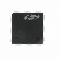
C8051F066-GQ Silicon Laboratories Inc, C8051F066-GQ Datasheet - Page 99

C8051F066-GQ
Manufacturer Part Number
C8051F066-GQ
Description
MCU 8-Bit C8051F06x 8051 CISC 32KB Flash 3.3V 100-Pin TQFP
Manufacturer
Silicon Laboratories Inc
Series
C8051F06xr
Specifications of C8051F066-GQ
Package
100TQFP
Device Core
8051
Family Name
C8051F06x
Maximum Speed
25 MHz
Operating Supply Voltage
3.3 V
Data Bus Width
8 Bit
Number Of Programmable I/os
59
Interface Type
I2C/SMBus/SPI/UART
On-chip Adc
2-chx16-bit
Number Of Timers
5
Ram Size
4.25 KB
Program Memory Size
32 KB
Program Memory Type
Flash
Operating Temperature
-40 to 85 °C
Core Processor
8051
Core Size
8-Bit
Speed
25MHz
Connectivity
EBI/EMI, SMBus (2-Wire/I²C), SPI, UART/USART
Peripherals
Brown-out Detect/Reset, POR, PWM, WDT
Number Of I /o
59
Voltage - Supply (vcc/vdd)
2.7 V ~ 3.6 V
Data Converters
A/D 2x16b
Oscillator Type
Internal
Package / Case
100-TQFP, 100-VQFP
Lead Free Status / RoHS Status
Lead free / RoHS Compliant
Eeprom Size
-
Lead Free Status / RoHS Status
Lead free / RoHS Compliant
Other names
336-1221
Available stocks
Company
Part Number
Manufacturer
Quantity
Price
Company:
Part Number:
C8051F066-GQ
Manufacturer:
Silicon Laboratories Inc
Quantity:
10 000
Company:
Part Number:
C8051F066-GQR
Manufacturer:
Silicon Laboratories Inc
Quantity:
10 000
- Current page: 99 of 328
- Download datasheet (2Mb)
7.3.1. Window Detector In Single-Ended Mode
Figure 7.15 shows two example window comparisons for right-justified, single-ended data, with
ADC2LTH:ADC2LTL = 0x0080 (128d) and ADC2GTH:ADC2GTL = 0x0040 (64d). In single-ended mode,
the input voltage can range from ‘0’ to VREF * (1023/1024) with respect to AGND, and is represented by a
10-bit unsigned integer value. In the left example, an AD2WINT interrupt will be generated if the ADC2
conversion word (ADC2H:ADC2L) is within the range defined by ADC2GTH:ADC2GTL and
ADC2LTH:ADC2LTL (if 0x0040 < ADC2H:ADC2L < 0x0080). In the right example, and AD2WINT interrupt
will be generated if the ADC2 conversion word is outside of the range defined by the ADC2GT and
ADC2LT registers (if ADC2H:ADC2L < 0x0040 or ADC2H:ADC2L > 0x0080). Figure 7.16 shows an exam-
ple using left-justified data with the same comparison values.
VREF x (1023/1024)
VREF x (1023/1024)
VREF x (128/1024)
VREF x (128/1024)
VREF x (64/1024)
VREF x (64/1024)
(P1.x - AGND)
(P1.x - AGND)
Input Voltage
Input Voltage
0
0
Figure 7.15. ADC Window Compare Example: Right-Justified Single-Ended Data
Figure 7.16. ADC Window Compare Example: Left-Justified Single-Ended Data
ADC2H:ADC2L
ADC2H:ADC2L
0xFFC0
0x03FF
0x007F
0x003F
0x1FC0
0x0FC0
0x0081
0x0080
0x0041
0x0040
0x0000
0x2040
0x2000
0x1040
0x1000
0x0000
ADC2GTH:ADC2GTL
ADC2GTH:ADC2GTL
ADC2LTH:ADC2LTL
ADC2LTH:ADC2LTL
not affected
not affected
not affected
not affected
AD2WINT
AD2WINT
AD2WINT
AD2WINT
AD2WINT=1
AD2WINT=1
Rev. 1.2
VREF x (1023/1024)
VREF x (1023/1024)
VREF x (128/1024)
VREF x (128/1024)
VREF x (64/1024)
VREF x (64/1024)
(P1.x - AGND)
(P1.x - AGND)
C8051F060/1/2/3/4/5/6/7
Input Voltage
Input Voltage
0
0
ADC2H:ADC2L
ADC2H:ADC2L
0xFFC0
0x03FF
0x0081
0x0080
0x007F
0x0041
0x0040
0x003F
0x0000
0x1FC0
0x0FC0
0x2040
0x2000
0x1040
0x1000
0x0000
ADC2GTH:ADC2GTL
ADC2GTH:ADC2GTL
ADC2LTH:ADC2LTL
ADC2LTH:ADC2LTL
not affected
not affected
AD2WINT
AD2WINT
AD2WINT=1
AD2WINT=1
AD2WINT=1
AD2WINT=1
99
Related parts for C8051F066-GQ
Image
Part Number
Description
Manufacturer
Datasheet
Request
R
Part Number:
Description:
SMD/C°/SINGLE-ENDED OUTPUT SILICON OSCILLATOR
Manufacturer:
Silicon Laboratories Inc
Part Number:
Description:
Manufacturer:
Silicon Laboratories Inc
Datasheet:
Part Number:
Description:
N/A N/A/SI4010 AES KEYFOB DEMO WITH LCD RX
Manufacturer:
Silicon Laboratories Inc
Datasheet:
Part Number:
Description:
N/A N/A/SI4010 SIMPLIFIED KEY FOB DEMO WITH LED RX
Manufacturer:
Silicon Laboratories Inc
Datasheet:
Part Number:
Description:
N/A/-40 TO 85 OC/EZLINK MODULE; F930/4432 HIGH BAND (REV E/B1)
Manufacturer:
Silicon Laboratories Inc
Part Number:
Description:
EZLink Module; F930/4432 Low Band (rev e/B1)
Manufacturer:
Silicon Laboratories Inc
Part Number:
Description:
I°/4460 10 DBM RADIO TEST CARD 434 MHZ
Manufacturer:
Silicon Laboratories Inc
Part Number:
Description:
I°/4461 14 DBM RADIO TEST CARD 868 MHZ
Manufacturer:
Silicon Laboratories Inc
Part Number:
Description:
I°/4463 20 DBM RFSWITCH RADIO TEST CARD 460 MHZ
Manufacturer:
Silicon Laboratories Inc
Part Number:
Description:
I°/4463 20 DBM RADIO TEST CARD 868 MHZ
Manufacturer:
Silicon Laboratories Inc
Part Number:
Description:
I°/4463 27 DBM RADIO TEST CARD 868 MHZ
Manufacturer:
Silicon Laboratories Inc
Part Number:
Description:
I°/4463 SKYWORKS 30 DBM RADIO TEST CARD 915 MHZ
Manufacturer:
Silicon Laboratories Inc
Part Number:
Description:
N/A N/A/-40 TO 85 OC/4463 RFMD 30 DBM RADIO TEST CARD 915 MHZ
Manufacturer:
Silicon Laboratories Inc
Part Number:
Description:
I°/4463 20 DBM RADIO TEST CARD 169 MHZ
Manufacturer:
Silicon Laboratories Inc


