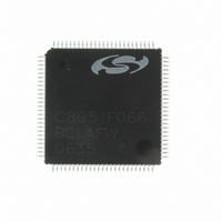
C8051F066-GQ Silicon Laboratories Inc, C8051F066-GQ Datasheet - Page 34

C8051F066-GQ
Manufacturer Part Number
C8051F066-GQ
Description
MCU 8-Bit C8051F06x 8051 CISC 32KB Flash 3.3V 100-Pin TQFP
Manufacturer
Silicon Laboratories Inc
Series
C8051F06xr
Specifications of C8051F066-GQ
Package
100TQFP
Device Core
8051
Family Name
C8051F06x
Maximum Speed
25 MHz
Operating Supply Voltage
3.3 V
Data Bus Width
8 Bit
Number Of Programmable I/os
59
Interface Type
I2C/SMBus/SPI/UART
On-chip Adc
2-chx16-bit
Number Of Timers
5
Ram Size
4.25 KB
Program Memory Size
32 KB
Program Memory Type
Flash
Operating Temperature
-40 to 85 °C
Core Processor
8051
Core Size
8-Bit
Speed
25MHz
Connectivity
EBI/EMI, SMBus (2-Wire/I²C), SPI, UART/USART
Peripherals
Brown-out Detect/Reset, POR, PWM, WDT
Number Of I /o
59
Voltage - Supply (vcc/vdd)
2.7 V ~ 3.6 V
Data Converters
A/D 2x16b
Oscillator Type
Internal
Package / Case
100-TQFP, 100-VQFP
Lead Free Status / RoHS Status
Lead free / RoHS Compliant
Eeprom Size
-
Lead Free Status / RoHS Status
Lead free / RoHS Compliant
Other names
336-1221
Available stocks
Company
Part Number
Manufacturer
Quantity
Price
Company:
Part Number:
C8051F066-GQ
Manufacturer:
Silicon Laboratories Inc
Quantity:
10 000
Company:
Part Number:
C8051F066-GQR
Manufacturer:
Silicon Laboratories Inc
Quantity:
10 000
- Current page: 34 of 328
- Download datasheet (2Mb)
C8051F060/1/2/3/4/5/6/7
1.9.
The C8051F060/1/2/3 devices have an on-board 10-bit SAR ADC (ADC2) with a 9-channel input multi-
plexer and programmable gain amplifier. This ADC features a 200 ksps maximum throughput and true 10-
bit performance with an INL of ±1LSB. Eight input pins are available for measurement and can be pro-
grammed as single-ended or differential inputs. Additionally, the on-chip temperature sensor can be used
as an input to the ADC. The ADC is under full control of the CIP-51 microcontroller via the Special Function
Registers. The ADC2 voltage reference is selected between the analog power supply (AV+) and the exter-
nal VREF2 pin. User software may put ADC2 into shutdown mode to save power.
A flexible conversion scheduling system allows ADC2 conversions to be initiated by software commands,
timer overflows, or an external input signal. Conversion completions are indicated by a status bit and an
interrupt (if enabled), and the resulting 10-bit data word is latched into two SFR locations upon completion.
ADC2 also contains Window Compare registers, which can be configured to interrupt the controller when
ADC2 data is within or outside of a specified range. ADC2 can monitor a key voltage continuously in back-
ground mode, and not interrupt the controller unless the converted data is within the specified window.
34
AIN2.0
AIN2.1
AIN2.2
AIN2.3
AIN2.4
AIN2.5
AIN2.6
AIN2.7
Differential Measurement
10-Bit Analog to Digital Converter
Single-ended or
AGND
Analog Multiplexer
SENSOR
TEMP
AMUX
9-to-1
Figure 1.13. 10-Bit ADC Diagram
VREF2 Pin
Configuration and Control Registers
AV+
Rev. 1.2
ADC
VREF
10-Bit
SAR
Start Conversion
10
ADC Data
Registers
10
Write to AD2BUSY
Timer 3 Overflow
CNVSTR2 Input
Timer 2 Overflow
Conversion
Compare
Complete
Window
Interrupt
ADC2
Logic
Related parts for C8051F066-GQ
Image
Part Number
Description
Manufacturer
Datasheet
Request
R
Part Number:
Description:
SMD/C°/SINGLE-ENDED OUTPUT SILICON OSCILLATOR
Manufacturer:
Silicon Laboratories Inc
Part Number:
Description:
Manufacturer:
Silicon Laboratories Inc
Datasheet:
Part Number:
Description:
N/A N/A/SI4010 AES KEYFOB DEMO WITH LCD RX
Manufacturer:
Silicon Laboratories Inc
Datasheet:
Part Number:
Description:
N/A N/A/SI4010 SIMPLIFIED KEY FOB DEMO WITH LED RX
Manufacturer:
Silicon Laboratories Inc
Datasheet:
Part Number:
Description:
N/A/-40 TO 85 OC/EZLINK MODULE; F930/4432 HIGH BAND (REV E/B1)
Manufacturer:
Silicon Laboratories Inc
Part Number:
Description:
EZLink Module; F930/4432 Low Band (rev e/B1)
Manufacturer:
Silicon Laboratories Inc
Part Number:
Description:
I°/4460 10 DBM RADIO TEST CARD 434 MHZ
Manufacturer:
Silicon Laboratories Inc
Part Number:
Description:
I°/4461 14 DBM RADIO TEST CARD 868 MHZ
Manufacturer:
Silicon Laboratories Inc
Part Number:
Description:
I°/4463 20 DBM RFSWITCH RADIO TEST CARD 460 MHZ
Manufacturer:
Silicon Laboratories Inc
Part Number:
Description:
I°/4463 20 DBM RADIO TEST CARD 868 MHZ
Manufacturer:
Silicon Laboratories Inc
Part Number:
Description:
I°/4463 27 DBM RADIO TEST CARD 868 MHZ
Manufacturer:
Silicon Laboratories Inc
Part Number:
Description:
I°/4463 SKYWORKS 30 DBM RADIO TEST CARD 915 MHZ
Manufacturer:
Silicon Laboratories Inc
Part Number:
Description:
N/A N/A/-40 TO 85 OC/4463 RFMD 30 DBM RADIO TEST CARD 915 MHZ
Manufacturer:
Silicon Laboratories Inc
Part Number:
Description:
I°/4463 20 DBM RADIO TEST CARD 169 MHZ
Manufacturer:
Silicon Laboratories Inc


