C8051F066-GQ Silicon Laboratories Inc, C8051F066-GQ Datasheet - Page 305
C8051F066-GQ
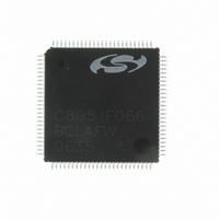
Manufacturer Part Number
C8051F066-GQ
Description
MCU 8-Bit C8051F06x 8051 CISC 32KB Flash 3.3V 100-Pin TQFP
Manufacturer
Silicon Laboratories Inc
Series
C8051F06xr
Specifications of C8051F066-GQ
Package
100TQFP
Device Core
8051
Family Name
C8051F06x
Maximum Speed
25 MHz
Operating Supply Voltage
3.3 V
Data Bus Width
8 Bit
Number Of Programmable I/os
59
Interface Type
I2C/SMBus/SPI/UART
On-chip Adc
2-chx16-bit
Number Of Timers
5
Ram Size
4.25 KB
Program Memory Size
32 KB
Program Memory Type
Flash
Operating Temperature
-40 to 85 °C
Core Processor
8051
Core Size
8-Bit
Speed
25MHz
Connectivity
EBI/EMI, SMBus (2-Wire/I²C), SPI, UART/USART
Peripherals
Brown-out Detect/Reset, POR, PWM, WDT
Number Of I /o
59
Voltage - Supply (vcc/vdd)
2.7 V ~ 3.6 V
Data Converters
A/D 2x16b
Oscillator Type
Internal
Package / Case
100-TQFP, 100-VQFP
Lead Free Status / RoHS Status
Lead free / RoHS Compliant
Eeprom Size
-
Lead Free Status / RoHS Status
Lead free / RoHS Compliant
Other names
336-1221
Available stocks
Company
Part Number
Manufacturer
Quantity
Price
Company:

Part Number:
C8051F066-GQ
Manufacturer:
Silicon Laboratories Inc
Quantity:
10 000
Company:
Part Number:
C8051F066-GQR
Manufacturer:
Silicon Laboratories Inc
Quantity:
10 000


25.2. Capture/Compare Modules
Each module can be configured to operate independently in one of six operation modes: Edge-triggered
Capture, Software Timer, High Speed Output, Frequency Output, 8-Bit Pulse Width Modulator, or 16-Bit
Pulse Width Modulator. Each module has Special Function Registers (SFRs) associated with it in the CIP-
51 system controller. These registers are used to exchange data with a module and configure the module's
mode of operation.
Table 25.2 summarizes the bit settings in the PCA0CPMn registers used to select the PCA0 capture/com-
pare module’s operating modes. Setting the ECCFn bit in a PCA0CPMn register enables the module's
CCFn interrupt. Note: PCA0 interrupts must be globally enabled before individual CCFn interrupts are rec-
ognized. PCA0 interrupts are globally enabled by setting the EA bit (IE.7) and the EPCA0 bit (EIE1.3) to
logic 1. See Figure 25.3 for details on the PCA interrupt configuration.
PWM16 ECOM CAPP CAPN
X
X
X
X
X
X
0
1
Timer Overflow
PCA Counter/
P
W
M
1
6
n
PCA Module 0
PCA Module 1
PCA Module 2
PCA Module 3
PCA Module 4
PCA Module 5
(for n = 0 to 5)
PCA0CPMn
E
C
O
M
n
X = Don’t Care
C
A
P
P
n
Table 25.2. PCA0CPM Register Settings for PCA Capture/Compare Modules
C
A
P
N
n
X
X
X
1
1
1
1
1
M
A
T
n
T
O
G
n
W
M
P
n
E
C
C
F
n
C
F
C
R
1
0
1
0
0
0
0
0
PCA0CN
C
C
F
5
C
C
F
4
C
C
F
3
C
C
F
2
C
C
F
1
C
C
F
0
0
1
1
0
0
0
0
0
Figure 25.3. PCA Interrupt Block Diagram
ECCF0
ECCF1
ECCF2
ECCF3
ECCF4
ECCF5
C
D
L
I
PCA0MD
C
P
S
MAT
2
C
P
S
1
0
0
0
1
1
0
0
0
0
1
0
1
0
1
0
1
0
1
0
1
C
P
S
0
C
E
F
0
1
TOG
0
0
0
0
1
1
0
0
Rev. 1.2
PWM ECCF
0
0
0
0
0
1
1
1
C8051F060/1/2/3/4/5/6/7
X
X
X
X
X
X
0
0
Capture triggered by positive edge on
CEXn
Capture triggered by negative edge on
CEXn
Capture triggered by transition on
CEXn
Software Timer
High Speed Output
Frequency Output
8-Bit Pulse Width Modulator
16-Bit Pulse Width Modulator
EPCA0
(EIE.3)
Operation Mode
0
1
(IE.7)
EA
0
1
Interrupt
Priority
Decoder
305
Related parts for C8051F066-GQ
Image
Part Number
Description
Manufacturer
Datasheet
Request
R

Part Number:
Description:
SMD/C°/SINGLE-ENDED OUTPUT SILICON OSCILLATOR
Manufacturer:
Silicon Laboratories Inc
Part Number:
Description:
Manufacturer:
Silicon Laboratories Inc
Datasheet:
Part Number:
Description:
N/A N/A/SI4010 AES KEYFOB DEMO WITH LCD RX
Manufacturer:
Silicon Laboratories Inc
Datasheet:
Part Number:
Description:
N/A N/A/SI4010 SIMPLIFIED KEY FOB DEMO WITH LED RX
Manufacturer:
Silicon Laboratories Inc
Datasheet:
Part Number:
Description:
N/A/-40 TO 85 OC/EZLINK MODULE; F930/4432 HIGH BAND (REV E/B1)
Manufacturer:
Silicon Laboratories Inc
Part Number:
Description:
EZLink Module; F930/4432 Low Band (rev e/B1)
Manufacturer:
Silicon Laboratories Inc
Part Number:
Description:
I°/4460 10 DBM RADIO TEST CARD 434 MHZ
Manufacturer:
Silicon Laboratories Inc
Part Number:
Description:
I°/4461 14 DBM RADIO TEST CARD 868 MHZ
Manufacturer:
Silicon Laboratories Inc
Part Number:
Description:
I°/4463 20 DBM RFSWITCH RADIO TEST CARD 460 MHZ
Manufacturer:
Silicon Laboratories Inc
Part Number:
Description:
I°/4463 20 DBM RADIO TEST CARD 868 MHZ
Manufacturer:
Silicon Laboratories Inc
Part Number:
Description:
I°/4463 27 DBM RADIO TEST CARD 868 MHZ
Manufacturer:
Silicon Laboratories Inc
Part Number:
Description:
I°/4463 SKYWORKS 30 DBM RADIO TEST CARD 915 MHZ
Manufacturer:
Silicon Laboratories Inc
Part Number:
Description:
N/A N/A/-40 TO 85 OC/4463 RFMD 30 DBM RADIO TEST CARD 915 MHZ
Manufacturer:
Silicon Laboratories Inc
Part Number:
Description:
I°/4463 20 DBM RADIO TEST CARD 169 MHZ
Manufacturer:
Silicon Laboratories Inc