C8051F066-GQ Silicon Laboratories Inc, C8051F066-GQ Datasheet - Page 82
C8051F066-GQ
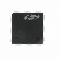
Manufacturer Part Number
C8051F066-GQ
Description
MCU 8-Bit C8051F06x 8051 CISC 32KB Flash 3.3V 100-Pin TQFP
Manufacturer
Silicon Laboratories Inc
Series
C8051F06xr
Specifications of C8051F066-GQ
Package
100TQFP
Device Core
8051
Family Name
C8051F06x
Maximum Speed
25 MHz
Operating Supply Voltage
3.3 V
Data Bus Width
8 Bit
Number Of Programmable I/os
59
Interface Type
I2C/SMBus/SPI/UART
On-chip Adc
2-chx16-bit
Number Of Timers
5
Ram Size
4.25 KB
Program Memory Size
32 KB
Program Memory Type
Flash
Operating Temperature
-40 to 85 °C
Core Processor
8051
Core Size
8-Bit
Speed
25MHz
Connectivity
EBI/EMI, SMBus (2-Wire/I²C), SPI, UART/USART
Peripherals
Brown-out Detect/Reset, POR, PWM, WDT
Number Of I /o
59
Voltage - Supply (vcc/vdd)
2.7 V ~ 3.6 V
Data Converters
A/D 2x16b
Oscillator Type
Internal
Package / Case
100-TQFP, 100-VQFP
Lead Free Status / RoHS Status
Lead free / RoHS Compliant
Eeprom Size
-
Lead Free Status / RoHS Status
Lead free / RoHS Compliant
Other names
336-1221
Available stocks
Company
Part Number
Manufacturer
Quantity
Price
Company:

Part Number:
C8051F066-GQ
Manufacturer:
Silicon Laboratories Inc
Quantity:
10 000
Company:
Part Number:
C8051F066-GQR
Manufacturer:
Silicon Laboratories Inc
Quantity:
10 000


C8051F060/1/2/3/4/5/6/7
82
Bits 7-6: Unused.
Bits 5-0: DMA0 instruction address to write (or read). When DMA0IDT is written or read, this register
Bit 7:
Bit 6:
Bit 5:
Bit 4:
Bits 3-0: RESERVED. Write to 0000b.
For more details on DMA instruction words, see
† This register points to a dedicated RAM location and its reset value is indeterminate.
SFR Page:
SFR Address:
SFR Page:
SFR Address:
CCNV
R/W
Bit7
Bit7
R
-
will be incremented to point to the next instruction address.
CCNV: Continuous Conversion.
0: Disable Continuous Conversion.
1: Enable Continuous Conversion. Repeat Counter value is ignored, and conversions will
continue.
DIFFSEL: Wait for data in differential mode.
0: Differential Data will not be collected.
1: Wait for differential data, and store to XRAM.
ADC1EN: Wait for data from ADC1.
0: ADC1 Data will not be collected.
1: Wait for ADC1 data, and store to XRAM.
ADC0EN: Wait for data from ADC0.
0: ADC0 Data will not be collected.
1: Wait for ADC0 data, and store to XRAM. If DIFFSEL is also ‘1’, only the differential data
will be stored.
3
0xDD
3
0xDE
DIFFSEL
R/W
Bit6
Bit6
R
-
Figure 6.6. DMA0IPT: DMA0 Instruction Write Address Register
Figure 6.7. DMA0IDT: DMA0 Instruction Write Data Register
ADC1EN
R/W
R/W
Bit5
Bit5
ADC0EN
R/W
R/W
Bit4
Bit4
Rev. 1.2
Section “6.2. DMA0 Instruction Format” on page
R/W
R/W
Bit3
Bit3
-
R/W
R/W
Bit2
Bit2
-
R/W
R/W
Bit1
Bit1
-
R/W
R/W
Bit0
Bit0
-
Reset Value†
Reset Value
00000000
xxxxxxxx
76.
Related parts for C8051F066-GQ
Image
Part Number
Description
Manufacturer
Datasheet
Request
R

Part Number:
Description:
SMD/C°/SINGLE-ENDED OUTPUT SILICON OSCILLATOR
Manufacturer:
Silicon Laboratories Inc
Part Number:
Description:
Manufacturer:
Silicon Laboratories Inc
Datasheet:
Part Number:
Description:
N/A N/A/SI4010 AES KEYFOB DEMO WITH LCD RX
Manufacturer:
Silicon Laboratories Inc
Datasheet:
Part Number:
Description:
N/A N/A/SI4010 SIMPLIFIED KEY FOB DEMO WITH LED RX
Manufacturer:
Silicon Laboratories Inc
Datasheet:
Part Number:
Description:
N/A/-40 TO 85 OC/EZLINK MODULE; F930/4432 HIGH BAND (REV E/B1)
Manufacturer:
Silicon Laboratories Inc
Part Number:
Description:
EZLink Module; F930/4432 Low Band (rev e/B1)
Manufacturer:
Silicon Laboratories Inc
Part Number:
Description:
I°/4460 10 DBM RADIO TEST CARD 434 MHZ
Manufacturer:
Silicon Laboratories Inc
Part Number:
Description:
I°/4461 14 DBM RADIO TEST CARD 868 MHZ
Manufacturer:
Silicon Laboratories Inc
Part Number:
Description:
I°/4463 20 DBM RFSWITCH RADIO TEST CARD 460 MHZ
Manufacturer:
Silicon Laboratories Inc
Part Number:
Description:
I°/4463 20 DBM RADIO TEST CARD 868 MHZ
Manufacturer:
Silicon Laboratories Inc
Part Number:
Description:
I°/4463 27 DBM RADIO TEST CARD 868 MHZ
Manufacturer:
Silicon Laboratories Inc
Part Number:
Description:
I°/4463 SKYWORKS 30 DBM RADIO TEST CARD 915 MHZ
Manufacturer:
Silicon Laboratories Inc
Part Number:
Description:
N/A N/A/-40 TO 85 OC/4463 RFMD 30 DBM RADIO TEST CARD 915 MHZ
Manufacturer:
Silicon Laboratories Inc
Part Number:
Description:
I°/4463 20 DBM RADIO TEST CARD 169 MHZ
Manufacturer:
Silicon Laboratories Inc