MCHC908GR8CFAE Freescale Semiconductor, MCHC908GR8CFAE Datasheet - Page 112
MCHC908GR8CFAE
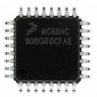
Manufacturer Part Number
MCHC908GR8CFAE
Description
IC MCU FLSH 8BIT8MHZ 7.5K32-LQFP
Manufacturer
Freescale Semiconductor
Series
HC08r
Specifications of MCHC908GR8CFAE
Core Processor
HC08
Core Size
8-Bit
Speed
8MHz
Connectivity
SCI, SPI
Peripherals
LVD, POR, PWM
Number Of I /o
21
Program Memory Size
7.5KB (7.5K x 8)
Program Memory Type
FLASH
Ram Size
384 x 8
Voltage - Supply (vcc/vdd)
2.7 V ~ 5.5 V
Data Converters
A/D 6x8b
Oscillator Type
Internal
Operating Temperature
-40°C ~ 85°C
Package / Case
32-LQFP
Controller Family/series
HC08
No. Of I/o's
21
Ram Memory Size
384Byte
Cpu Speed
8MHz
No. Of Timers
2
Embedded Interface Type
I2C, SCI, SPI
Rohs Compliant
Yes
Processor Series
HC08G
Core
HC08
Data Bus Width
8 bit
Data Ram Size
384 B
Interface Type
SCI, SPI
Maximum Clock Frequency
8.2 MHz
Number Of Programmable I/os
21
Number Of Timers
3
Operating Supply Voltage
2.7 V to 5.5 V
Maximum Operating Temperature
+ 85 C
Mounting Style
SMD/SMT
Development Tools By Supplier
FSICEBASE, DEMO908GZ60E, M68CBL05CE, M68EML08GPGTE
Minimum Operating Temperature
- 40 C
On-chip Adc
8 bit, 6 Channel
Lead Free Status / RoHS Status
Lead free / RoHS Compliant
Eeprom Size
-
Lead Free Status / Rohs Status
Details
Available stocks
Company
Part Number
Manufacturer
Quantity
Price

Company:
Part Number:
MCHC908GR8CFAE
Manufacturer:
Freescale Semiconductor
Quantity:
10 000
Company:
Part Number:
MCHC908GR8CFAER
Manufacturer:
Freescale Semiconductor
Quantity:
10 000


Clock Generator Module (CGMC)
7.5 I/O Signals
7.5.1 Crystal Amplifier Input Pin (OSC1)
7.5.2 Crystal Amplifier Output Pin (OSC2)
7.5.3 External Filter Capacitor Pin (CGMXFC)
7.5.4 PLL Analog Power Pin (V
7.5.5 PLL Analog Ground Pin (V
Technical Data
112
NOTE:
NOTE:
NOTE:
The following paragraphs describe the CGMC I/O signals.
The OSC1 pin is an input to the crystal oscillator amplifier.
The OSC2 pin is the output of the crystal oscillator inverting amplifier.
The CGMXFC pin is required by the loop filter to filter out phase
corrections. An external filter network is connected to this pin. (See
Figure
To prevent noise problems, the filter network should be placed as close
to the CGMXFC pin as possible, with minimum routing distances and no
routing of other signals across the network.
V
V
Route V
capacitors as close as possible to the package.
V
the V
Route V
capacitors as close as possible to the package.
DDA
DDA
SSA
Freescale Semiconductor, Inc.
For More Information On This Product,
SSA
is a ground pin used by the analog portions of the PLL. Connect
is a power pin used by the analog portions of the PLL. Connect the
pin to the same voltage potential as the V
7-2.)
DDA
SSA
pin to the same voltage potential as the V
DDA
Clock Generator Module (CGMC)
SSA
carefully for maximum noise immunity and place bypass
Go to: www.freescale.com
carefully for maximum noise immunity and place bypass
)
)
MC68HC908GR8 — Rev 4.0
DD
pin.
SS
pin.
MOTOROLA
Related parts for MCHC908GR8CFAE
Image
Part Number
Description
Manufacturer
Datasheet
Request
R

Part Number:
Description:
Manufacturer:
Freescale Semiconductor, Inc
Datasheet:
Part Number:
Description:
Manufacturer:
Freescale Semiconductor, Inc
Datasheet:
Part Number:
Description:
Manufacturer:
Freescale Semiconductor, Inc
Datasheet:
Part Number:
Description:
Manufacturer:
Freescale Semiconductor, Inc
Datasheet:
Part Number:
Description:
Manufacturer:
Freescale Semiconductor, Inc
Datasheet:
Part Number:
Description:
Manufacturer:
Freescale Semiconductor, Inc
Datasheet:
Part Number:
Description:
Manufacturer:
Freescale Semiconductor, Inc
Datasheet:
Part Number:
Description:
Manufacturer:
Freescale Semiconductor, Inc
Datasheet:
Part Number:
Description:
Manufacturer:
Freescale Semiconductor, Inc
Datasheet:
Part Number:
Description:
Manufacturer:
Freescale Semiconductor, Inc
Datasheet:
Part Number:
Description:
Manufacturer:
Freescale Semiconductor, Inc
Datasheet:
Part Number:
Description:
Manufacturer:
Freescale Semiconductor, Inc
Datasheet:
Part Number:
Description:
Manufacturer:
Freescale Semiconductor, Inc
Datasheet:
Part Number:
Description:
Manufacturer:
Freescale Semiconductor, Inc
Datasheet:
Part Number:
Description:
Manufacturer:
Freescale Semiconductor, Inc
Datasheet: