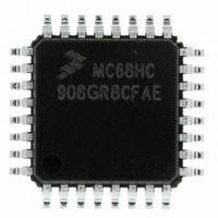
MCHC908GR8CFAE Freescale Semiconductor, MCHC908GR8CFAE Datasheet - Page 303

MCHC908GR8CFAE
Manufacturer Part Number
MCHC908GR8CFAE
Description
IC MCU FLSH 8BIT8MHZ 7.5K32-LQFP
Manufacturer
Freescale Semiconductor
Series
HC08r
Specifications of MCHC908GR8CFAE
Core Processor
HC08
Core Size
8-Bit
Speed
8MHz
Connectivity
SCI, SPI
Peripherals
LVD, POR, PWM
Number Of I /o
21
Program Memory Size
7.5KB (7.5K x 8)
Program Memory Type
FLASH
Ram Size
384 x 8
Voltage - Supply (vcc/vdd)
2.7 V ~ 5.5 V
Data Converters
A/D 6x8b
Oscillator Type
Internal
Operating Temperature
-40°C ~ 85°C
Package / Case
32-LQFP
Controller Family/series
HC08
No. Of I/o's
21
Ram Memory Size
384Byte
Cpu Speed
8MHz
No. Of Timers
2
Embedded Interface Type
I2C, SCI, SPI
Rohs Compliant
Yes
Processor Series
HC08G
Core
HC08
Data Bus Width
8 bit
Data Ram Size
384 B
Interface Type
SCI, SPI
Maximum Clock Frequency
8.2 MHz
Number Of Programmable I/os
21
Number Of Timers
3
Operating Supply Voltage
2.7 V to 5.5 V
Maximum Operating Temperature
+ 85 C
Mounting Style
SMD/SMT
Development Tools By Supplier
FSICEBASE, DEMO908GZ60E, M68CBL05CE, M68EML08GPGTE
Minimum Operating Temperature
- 40 C
On-chip Adc
8 bit, 6 Channel
Lead Free Status / RoHS Status
Lead free / RoHS Compliant
Eeprom Size
-
Lead Free Status / Rohs Status
Details
Available stocks
Company
Part Number
Manufacturer
Quantity
Price
Company:
Part Number:
MCHC908GR8CFAE
Manufacturer:
Freescale Semiconductor
Quantity:
10 000
Company:
Part Number:
MCHC908GR8CFAER
Manufacturer:
Freescale Semiconductor
Quantity:
10 000
- Current page: 303 of 408
- Download datasheet (4Mb)
20.6 Transmission Formats
20.6.1 Clock Phase and Polarity Controls
MC68HC908GR8 — Rev 4.0
MOTOROLA
NOTE:
When the master SPI starts a transmission, the data in the slave shift
register begins shifting out on the MISO pin. The slave can load its shift
register with a new byte for the next transmission by writing to its transmit
data register. The slave must write to its transmit data register at least
one bus cycle before the master starts the next transmission. Otherwise,
the byte already in the slave shift register shifts out on the MISO pin.
Data written to the slave shift register during a transmission remains in
a buffer until the end of the transmission.
When the clock phase bit (CPHA) is set, the first edge of SPSCK starts
a transmission. When CPHA is clear, the falling edge of SS starts a
transmission. See
SPSCK must be in the proper idle state before the slave is enabled to
prevent SPSCK from appearing as a clock edge.
During an SPI transmission, data is simultaneously transmitted (shifted
out serially) and received (shifted in serially). A serial clock synchronizes
shifting and sampling on the two serial data lines. A slave select line
allows selection of an individual slave SPI device; slave devices that are
not selected do not interfere with SPI bus activities. On a master SPI
device, the slave select line can optionally be used to indicate multiple-
master bus contention.
Software can select any of four combinations of serial clock (SPSCK)
phase and polarity using two bits in the SPI control register (SPCR). The
clock polarity is specified by the CPOL control bit, which selects an
active high or low clock and has no significant effect on the transmission
format.
Freescale Semiconductor, Inc.
For More Information On This Product,
Serial Peripheral Interface (SPI)
Go to: www.freescale.com
Transmission
Formats.
Serial Peripheral Interface (SPI)
Transmission Formats
Technical Data
303
Related parts for MCHC908GR8CFAE
Image
Part Number
Description
Manufacturer
Datasheet
Request
R
Part Number:
Description:
Manufacturer:
Freescale Semiconductor, Inc
Datasheet:
Part Number:
Description:
Manufacturer:
Freescale Semiconductor, Inc
Datasheet:
Part Number:
Description:
Manufacturer:
Freescale Semiconductor, Inc
Datasheet:
Part Number:
Description:
Manufacturer:
Freescale Semiconductor, Inc
Datasheet:
Part Number:
Description:
Manufacturer:
Freescale Semiconductor, Inc
Datasheet:
Part Number:
Description:
Manufacturer:
Freescale Semiconductor, Inc
Datasheet:
Part Number:
Description:
Manufacturer:
Freescale Semiconductor, Inc
Datasheet:
Part Number:
Description:
Manufacturer:
Freescale Semiconductor, Inc
Datasheet:
Part Number:
Description:
Manufacturer:
Freescale Semiconductor, Inc
Datasheet:
Part Number:
Description:
Manufacturer:
Freescale Semiconductor, Inc
Datasheet:
Part Number:
Description:
Manufacturer:
Freescale Semiconductor, Inc
Datasheet:
Part Number:
Description:
Manufacturer:
Freescale Semiconductor, Inc
Datasheet:
Part Number:
Description:
Manufacturer:
Freescale Semiconductor, Inc
Datasheet:
Part Number:
Description:
Manufacturer:
Freescale Semiconductor, Inc
Datasheet:
Part Number:
Description:
Manufacturer:
Freescale Semiconductor, Inc
Datasheet:


