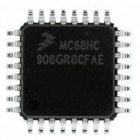
MCHC908GR8CFAE Freescale Semiconductor, MCHC908GR8CFAE Datasheet - Page 213

MCHC908GR8CFAE
Manufacturer Part Number
MCHC908GR8CFAE
Description
IC MCU FLSH 8BIT8MHZ 7.5K32-LQFP
Manufacturer
Freescale Semiconductor
Series
HC08r
Specifications of MCHC908GR8CFAE
Core Processor
HC08
Core Size
8-Bit
Speed
8MHz
Connectivity
SCI, SPI
Peripherals
LVD, POR, PWM
Number Of I /o
21
Program Memory Size
7.5KB (7.5K x 8)
Program Memory Type
FLASH
Ram Size
384 x 8
Voltage - Supply (vcc/vdd)
2.7 V ~ 5.5 V
Data Converters
A/D 6x8b
Oscillator Type
Internal
Operating Temperature
-40°C ~ 85°C
Package / Case
32-LQFP
Controller Family/series
HC08
No. Of I/o's
21
Ram Memory Size
384Byte
Cpu Speed
8MHz
No. Of Timers
2
Embedded Interface Type
I2C, SCI, SPI
Rohs Compliant
Yes
Processor Series
HC08G
Core
HC08
Data Bus Width
8 bit
Data Ram Size
384 B
Interface Type
SCI, SPI
Maximum Clock Frequency
8.2 MHz
Number Of Programmable I/os
21
Number Of Timers
3
Operating Supply Voltage
2.7 V to 5.5 V
Maximum Operating Temperature
+ 85 C
Mounting Style
SMD/SMT
Development Tools By Supplier
FSICEBASE, DEMO908GZ60E, M68CBL05CE, M68EML08GPGTE
Minimum Operating Temperature
- 40 C
On-chip Adc
8 bit, 6 Channel
Lead Free Status / RoHS Status
Lead free / RoHS Compliant
Eeprom Size
-
Lead Free Status / Rohs Status
Details
Available stocks
Company
Part Number
Manufacturer
Quantity
Price
Company:
Part Number:
MCHC908GR8CFAE
Manufacturer:
Freescale Semiconductor
Quantity:
10 000
Company:
Part Number:
MCHC908GR8CFAER
Manufacturer:
Freescale Semiconductor
Quantity:
10 000
- Current page: 213 of 408
- Download datasheet (4Mb)
16.4 Port B
16.4.1 Port B Data Register
MC68HC908GR8 — Rev 4.0
MOTOROLA
NOTE:
NOTE:
Function:
Alternate
Address:
Port B is an 6-bit special-function port that shares all six of its pins with
the analog-to-digital converter (ADC) module.
The port B data register (PTB) contains a data latch for each of the six
port pins.
PTB5–PTB0 — Port B Data Bits
AD5–AD0 — Analog-to-Digital Input Bits
Care must be taken when reading port B while applying analog voltages
to AD5–AD0 pins. If the appropriate ADC channel is not enabled,
excessive current drain may occur if analog voltages are applied to the
PTBx/ADx pin, while PTB is read as a digital input. Those ports not
selected as analog input channels are considered digital I/O ports.
PTB4 and 5 are not available in a 28-pin DIP and SOIC package
Reset:
Read:
Write:
Freescale Semiconductor, Inc.
These read/write bits are software-programmable. Data direction of
each port B pin is under the control of the corresponding bit in data
direction register B. Reset has no effect on port B data.
AD5–AD0 are pins used for the input channels to the analog-to-digital
converter module. The channel select bits in the ADC status and
control register define which port B pin will be used as an ADC input
and overrides any control from the port I/O logic by forcing that pin as
the input to the analog circuitry.
For More Information On This Product,
$0001
Bit 7
0
Go to: www.freescale.com
Figure 16-6. Port B Data Register (PTB)
Input/Output Ports (I/O)
6
0
PTB5
AD5
5
Unaffected by reset
PTB4
AD4
4
PTB3
AD3
3
PTB2
AD2
2
Input/Output Ports (I/O)
PTB1
AD1
1
Technical Data
PTB0
Bit 0
AD0
Port B
213
Related parts for MCHC908GR8CFAE
Image
Part Number
Description
Manufacturer
Datasheet
Request
R
Part Number:
Description:
Manufacturer:
Freescale Semiconductor, Inc
Datasheet:
Part Number:
Description:
Manufacturer:
Freescale Semiconductor, Inc
Datasheet:
Part Number:
Description:
Manufacturer:
Freescale Semiconductor, Inc
Datasheet:
Part Number:
Description:
Manufacturer:
Freescale Semiconductor, Inc
Datasheet:
Part Number:
Description:
Manufacturer:
Freescale Semiconductor, Inc
Datasheet:
Part Number:
Description:
Manufacturer:
Freescale Semiconductor, Inc
Datasheet:
Part Number:
Description:
Manufacturer:
Freescale Semiconductor, Inc
Datasheet:
Part Number:
Description:
Manufacturer:
Freescale Semiconductor, Inc
Datasheet:
Part Number:
Description:
Manufacturer:
Freescale Semiconductor, Inc
Datasheet:
Part Number:
Description:
Manufacturer:
Freescale Semiconductor, Inc
Datasheet:
Part Number:
Description:
Manufacturer:
Freescale Semiconductor, Inc
Datasheet:
Part Number:
Description:
Manufacturer:
Freescale Semiconductor, Inc
Datasheet:
Part Number:
Description:
Manufacturer:
Freescale Semiconductor, Inc
Datasheet:
Part Number:
Description:
Manufacturer:
Freescale Semiconductor, Inc
Datasheet:
Part Number:
Description:
Manufacturer:
Freescale Semiconductor, Inc
Datasheet:


