MCHC908GR8CFAE Freescale Semiconductor, MCHC908GR8CFAE Datasheet - Page 121
MCHC908GR8CFAE
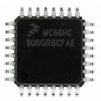
Manufacturer Part Number
MCHC908GR8CFAE
Description
IC MCU FLSH 8BIT8MHZ 7.5K32-LQFP
Manufacturer
Freescale Semiconductor
Series
HC08r
Specifications of MCHC908GR8CFAE
Core Processor
HC08
Core Size
8-Bit
Speed
8MHz
Connectivity
SCI, SPI
Peripherals
LVD, POR, PWM
Number Of I /o
21
Program Memory Size
7.5KB (7.5K x 8)
Program Memory Type
FLASH
Ram Size
384 x 8
Voltage - Supply (vcc/vdd)
2.7 V ~ 5.5 V
Data Converters
A/D 6x8b
Oscillator Type
Internal
Operating Temperature
-40°C ~ 85°C
Package / Case
32-LQFP
Controller Family/series
HC08
No. Of I/o's
21
Ram Memory Size
384Byte
Cpu Speed
8MHz
No. Of Timers
2
Embedded Interface Type
I2C, SCI, SPI
Rohs Compliant
Yes
Processor Series
HC08G
Core
HC08
Data Bus Width
8 bit
Data Ram Size
384 B
Interface Type
SCI, SPI
Maximum Clock Frequency
8.2 MHz
Number Of Programmable I/os
21
Number Of Timers
3
Operating Supply Voltage
2.7 V to 5.5 V
Maximum Operating Temperature
+ 85 C
Mounting Style
SMD/SMT
Development Tools By Supplier
FSICEBASE, DEMO908GZ60E, M68CBL05CE, M68EML08GPGTE
Minimum Operating Temperature
- 40 C
On-chip Adc
8 bit, 6 Channel
Lead Free Status / RoHS Status
Lead free / RoHS Compliant
Eeprom Size
-
Lead Free Status / Rohs Status
Details
Available stocks
Company
Part Number
Manufacturer
Quantity
Price

Company:
Part Number:
MCHC908GR8CFAE
Manufacturer:
Freescale Semiconductor
Quantity:
10 000
Company:
Part Number:
MCHC908GR8CFAER
Manufacturer:
Freescale Semiconductor
Quantity:
10 000


7.6.5 PLL VCO Range Select Register
MC68HC908GR8 — Rev 4.0
MOTOROLA
NOTE:
NOTE:
Address:
PMRS may be called PVRS on other HC08 derivatives.
The PLL VCO range select register (PMRS) contains the programming
information required for the hardware configuration of the VCO.
VRS7–VRS0 — VCO Range Select Bits
The VCO range select bits have built-in protection such that they cannot
be written when the PLL is on (PLLON = 1) and such that the VCO clock
cannot be selected as the source of the base clock (BCS = 1) if the VCO
range select bits are all clear.
The PLL VCO range select register must be programmed correctly.
Incorrect programming can result in failure of the PLL to achieve lock.
Reset:
Read:
Write:
Freescale Semiconductor, Inc.
These read/write bits control the hardware center-of-range linear
multiplier L which, in conjunction with E (see
Programming the
hardware center-of-range frequency, f
written when the PLLON bit in the PCTL is set. (See
Programming
register disables the PLL and clears the BCS bit in the PLL control
register (PCTL). (See
Programming
default range multiply value of 64.
For More Information On This Product,
Figure 7-8. PLL VCO Range Select Register (PMRS)
$003A
VRS7
Bit 7
0
Clock Generator Module (CGMC)
Go to: www.freescale.com
VRS6
Exceptions.) A value of $00 in the VCO range select
Exceptions.). Reset initializes the register to $40 for a
6
1
PLL, and
VRS5
Base Clock Selector Circuit
5
0
PLL Control
VRS4
4
0
VRS
VRS3
3
0
Register), controls the
Clock Generator Module (CGMC)
. VRS7–VRS0 cannot be
PLL
VRS2
2
0
Circuits,
and
Special
CGMC Registers
VRS1
Special
1
0
Technical Data
VRS0
Bit 0
0
121
Related parts for MCHC908GR8CFAE
Image
Part Number
Description
Manufacturer
Datasheet
Request
R

Part Number:
Description:
Manufacturer:
Freescale Semiconductor, Inc
Datasheet:
Part Number:
Description:
Manufacturer:
Freescale Semiconductor, Inc
Datasheet:
Part Number:
Description:
Manufacturer:
Freescale Semiconductor, Inc
Datasheet:
Part Number:
Description:
Manufacturer:
Freescale Semiconductor, Inc
Datasheet:
Part Number:
Description:
Manufacturer:
Freescale Semiconductor, Inc
Datasheet:
Part Number:
Description:
Manufacturer:
Freescale Semiconductor, Inc
Datasheet:
Part Number:
Description:
Manufacturer:
Freescale Semiconductor, Inc
Datasheet:
Part Number:
Description:
Manufacturer:
Freescale Semiconductor, Inc
Datasheet:
Part Number:
Description:
Manufacturer:
Freescale Semiconductor, Inc
Datasheet:
Part Number:
Description:
Manufacturer:
Freescale Semiconductor, Inc
Datasheet:
Part Number:
Description:
Manufacturer:
Freescale Semiconductor, Inc
Datasheet:
Part Number:
Description:
Manufacturer:
Freescale Semiconductor, Inc
Datasheet:
Part Number:
Description:
Manufacturer:
Freescale Semiconductor, Inc
Datasheet:
Part Number:
Description:
Manufacturer:
Freescale Semiconductor, Inc
Datasheet:
Part Number:
Description:
Manufacturer:
Freescale Semiconductor, Inc
Datasheet: