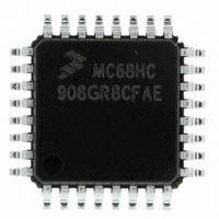
MCHC908GR8CFAE Freescale Semiconductor, MCHC908GR8CFAE Datasheet - Page 221

MCHC908GR8CFAE
Manufacturer Part Number
MCHC908GR8CFAE
Description
IC MCU FLSH 8BIT8MHZ 7.5K32-LQFP
Manufacturer
Freescale Semiconductor
Series
HC08r
Specifications of MCHC908GR8CFAE
Core Processor
HC08
Core Size
8-Bit
Speed
8MHz
Connectivity
SCI, SPI
Peripherals
LVD, POR, PWM
Number Of I /o
21
Program Memory Size
7.5KB (7.5K x 8)
Program Memory Type
FLASH
Ram Size
384 x 8
Voltage - Supply (vcc/vdd)
2.7 V ~ 5.5 V
Data Converters
A/D 6x8b
Oscillator Type
Internal
Operating Temperature
-40°C ~ 85°C
Package / Case
32-LQFP
Controller Family/series
HC08
No. Of I/o's
21
Ram Memory Size
384Byte
Cpu Speed
8MHz
No. Of Timers
2
Embedded Interface Type
I2C, SCI, SPI
Rohs Compliant
Yes
Processor Series
HC08G
Core
HC08
Data Bus Width
8 bit
Data Ram Size
384 B
Interface Type
SCI, SPI
Maximum Clock Frequency
8.2 MHz
Number Of Programmable I/os
21
Number Of Timers
3
Operating Supply Voltage
2.7 V to 5.5 V
Maximum Operating Temperature
+ 85 C
Mounting Style
SMD/SMT
Development Tools By Supplier
FSICEBASE, DEMO908GZ60E, M68CBL05CE, M68EML08GPGTE
Minimum Operating Temperature
- 40 C
On-chip Adc
8 bit, 6 Channel
Lead Free Status / RoHS Status
Lead free / RoHS Compliant
Eeprom Size
-
Lead Free Status / Rohs Status
Details
Available stocks
Company
Part Number
Manufacturer
Quantity
Price
Company:
Part Number:
MCHC908GR8CFAE
Manufacturer:
Freescale Semiconductor
Quantity:
10 000
Company:
Part Number:
MCHC908GR8CFAER
Manufacturer:
Freescale Semiconductor
Quantity:
10 000
- Current page: 221 of 408
- Download datasheet (4Mb)
MC68HC908GR8 — Rev 4.0
MOTOROLA
T1CH1 and T1CH0 — Timer 1 Channel I/O Bits
SPSCK — SPI Serial Clock
MOSI — Master Out/Slave In
MISO — Master In/Slave Out
SS — Slave Select
Freescale Semiconductor, Inc.
The PTD5/T1CH1–PTD4/T1CH0 pins are the TIM1 input
capture/output compare pins. The edge/level select bits, ELSxB and
ELSxA, determine whether the PTD5/T1CH1–PTD4/T1CH0 pins are
timer channel I/O pins or general-purpose I/O pins. See
Interface Module
The PTD3/SPSCK pin is the serial clock input of the SPI module.
When the SPE bit is clear, the PTD3/SPSCK pin is available for
general-purpose I/O.
The PTD2/MOSI pin is the master out/slave in terminal of the SPI
module. When the SPE bit is clear, the PTD2/MOSI pin is available
for general-purpose I/O.
The PTD1/MISO pin is the master in/slave out terminal of the SPI
module. When the SPI enable bit, SPE, is clear, the SPI module is
disabled, and the PTD0/SS pin is available for general-purpose I/O.
Data direction register D (DDRD) does not affect the data direction of
port D pins that are being used by the SPI module. However, the
DDRD bits always determine whether reading port D returns the
states of the latches or the states of the pins. See
The PTD0/SS pin is the slave select input of the SPI module. When
the SPE bit is clear, or when the SPI master bit, SPMSTR, is set, the
PTD0/SS pin is available for general-purpose I/O. When the SPI is
enabled, the DDRB0 bit in data direction register B (DDRB) has no
effect on the PTD0/SS pin.
For More Information On This Product,
Go to: www.freescale.com
Input/Output Ports (I/O)
(TIM).
Input/Output Ports (I/O)
Table
Timer
Technical Data
16-5.
Port D
221
Related parts for MCHC908GR8CFAE
Image
Part Number
Description
Manufacturer
Datasheet
Request
R
Part Number:
Description:
Manufacturer:
Freescale Semiconductor, Inc
Datasheet:
Part Number:
Description:
Manufacturer:
Freescale Semiconductor, Inc
Datasheet:
Part Number:
Description:
Manufacturer:
Freescale Semiconductor, Inc
Datasheet:
Part Number:
Description:
Manufacturer:
Freescale Semiconductor, Inc
Datasheet:
Part Number:
Description:
Manufacturer:
Freescale Semiconductor, Inc
Datasheet:
Part Number:
Description:
Manufacturer:
Freescale Semiconductor, Inc
Datasheet:
Part Number:
Description:
Manufacturer:
Freescale Semiconductor, Inc
Datasheet:
Part Number:
Description:
Manufacturer:
Freescale Semiconductor, Inc
Datasheet:
Part Number:
Description:
Manufacturer:
Freescale Semiconductor, Inc
Datasheet:
Part Number:
Description:
Manufacturer:
Freescale Semiconductor, Inc
Datasheet:
Part Number:
Description:
Manufacturer:
Freescale Semiconductor, Inc
Datasheet:
Part Number:
Description:
Manufacturer:
Freescale Semiconductor, Inc
Datasheet:
Part Number:
Description:
Manufacturer:
Freescale Semiconductor, Inc
Datasheet:
Part Number:
Description:
Manufacturer:
Freescale Semiconductor, Inc
Datasheet:
Part Number:
Description:
Manufacturer:
Freescale Semiconductor, Inc
Datasheet:


