MCHC908GR8CFAE Freescale Semiconductor, MCHC908GR8CFAE Datasheet - Page 186
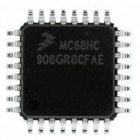
MCHC908GR8CFAE
Manufacturer Part Number
MCHC908GR8CFAE
Description
IC MCU FLSH 8BIT8MHZ 7.5K32-LQFP
Manufacturer
Freescale Semiconductor
Series
HC08r
Specifications of MCHC908GR8CFAE
Core Processor
HC08
Core Size
8-Bit
Speed
8MHz
Connectivity
SCI, SPI
Peripherals
LVD, POR, PWM
Number Of I /o
21
Program Memory Size
7.5KB (7.5K x 8)
Program Memory Type
FLASH
Ram Size
384 x 8
Voltage - Supply (vcc/vdd)
2.7 V ~ 5.5 V
Data Converters
A/D 6x8b
Oscillator Type
Internal
Operating Temperature
-40°C ~ 85°C
Package / Case
32-LQFP
Controller Family/series
HC08
No. Of I/o's
21
Ram Memory Size
384Byte
Cpu Speed
8MHz
No. Of Timers
2
Embedded Interface Type
I2C, SCI, SPI
Rohs Compliant
Yes
Processor Series
HC08G
Core
HC08
Data Bus Width
8 bit
Data Ram Size
384 B
Interface Type
SCI, SPI
Maximum Clock Frequency
8.2 MHz
Number Of Programmable I/os
21
Number Of Timers
3
Operating Supply Voltage
2.7 V to 5.5 V
Maximum Operating Temperature
+ 85 C
Mounting Style
SMD/SMT
Development Tools By Supplier
FSICEBASE, DEMO908GZ60E, M68CBL05CE, M68EML08GPGTE
Minimum Operating Temperature
- 40 C
On-chip Adc
8 bit, 6 Channel
Lead Free Status / RoHS Status
Lead free / RoHS Compliant
Eeprom Size
-
Lead Free Status / Rohs Status
Details
Available stocks
Company
Part Number
Manufacturer
Quantity
Price

Company:
Part Number:
MCHC908GR8CFAE
Manufacturer:
Freescale Semiconductor
Quantity:
10 000
Company:
Part Number:
MCHC908GR8CFAER
Manufacturer:
Freescale Semiconductor
Quantity:
10 000


Low-Voltage Inhibit (LVI)
14.4.1 Polled LVI Operation
14.4.2 Forced Reset Operation
14.4.3 Voltage Hysteresis Protection
Technical Data
186
Addr.
$FE0C
Register Name
LVI Status Register
(LVISR)
In applications that can operate at V
software can monitor V
register, the LVIPWRD bit must be at logic 0 to enable the LVI module,
and the LVIRSTD bit must be at logic 1 to disable LVI resets.
In applications that require V
enabling LVI resets allows the LVI module to reset the MCU when V
falls below the V
and LVIRSTD bits must be at logic 0 to enable the LVI module and to
enable LVI resets.
Once the LVI has triggered (by having V
will maintain a reset condition until V
voltage, V
continually entering and exiting reset if V
V
Reset:
Read: LVIOUT
TRIPF
Write:
Freescale Semiconductor, Inc.
Figure 14-2. LVI I/O Register Summary
For More Information On This Product,
. V
Bit 7
TRIPR
0
TRIPR
Go to: www.freescale.com
Low-Voltage Inhibit (LVI)
= Unimplemented
. This prevents a condition in which the MCU is
is greater than V
TRIPF
6
0
0
level. In the configuration register, the LVIPWRD
DD
5
by polling the LVIOUT bit. In the configuration
0
0
DD
to remain above the V
TRIPF
4
0
0
DD
DD
by the hysteresis voltage, V
levels below the V
rises above the rising trip point
DD
DD
3
0
0
fall below V
is approximately equal to
MC68HC908GR8 — Rev 4.0
2
0
0
TRIPF
TRIPF
TRIPF
1
0
0
level,
), the LVI
MOTOROLA
level,
Bit 0
HYS
0
0
DD
.
Related parts for MCHC908GR8CFAE
Image
Part Number
Description
Manufacturer
Datasheet
Request
R

Part Number:
Description:
Manufacturer:
Freescale Semiconductor, Inc
Datasheet:
Part Number:
Description:
Manufacturer:
Freescale Semiconductor, Inc
Datasheet:
Part Number:
Description:
Manufacturer:
Freescale Semiconductor, Inc
Datasheet:
Part Number:
Description:
Manufacturer:
Freescale Semiconductor, Inc
Datasheet:
Part Number:
Description:
Manufacturer:
Freescale Semiconductor, Inc
Datasheet:
Part Number:
Description:
Manufacturer:
Freescale Semiconductor, Inc
Datasheet:
Part Number:
Description:
Manufacturer:
Freescale Semiconductor, Inc
Datasheet:
Part Number:
Description:
Manufacturer:
Freescale Semiconductor, Inc
Datasheet:
Part Number:
Description:
Manufacturer:
Freescale Semiconductor, Inc
Datasheet:
Part Number:
Description:
Manufacturer:
Freescale Semiconductor, Inc
Datasheet:
Part Number:
Description:
Manufacturer:
Freescale Semiconductor, Inc
Datasheet:
Part Number:
Description:
Manufacturer:
Freescale Semiconductor, Inc
Datasheet:
Part Number:
Description:
Manufacturer:
Freescale Semiconductor, Inc
Datasheet:
Part Number:
Description:
Manufacturer:
Freescale Semiconductor, Inc
Datasheet:
Part Number:
Description:
Manufacturer:
Freescale Semiconductor, Inc
Datasheet: