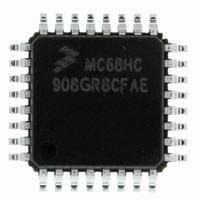
MCHC908GR8CFAE Freescale Semiconductor, MCHC908GR8CFAE Datasheet - Page 88

MCHC908GR8CFAE
Manufacturer Part Number
MCHC908GR8CFAE
Description
IC MCU FLSH 8BIT8MHZ 7.5K32-LQFP
Manufacturer
Freescale Semiconductor
Series
HC08r
Specifications of MCHC908GR8CFAE
Core Processor
HC08
Core Size
8-Bit
Speed
8MHz
Connectivity
SCI, SPI
Peripherals
LVD, POR, PWM
Number Of I /o
21
Program Memory Size
7.5KB (7.5K x 8)
Program Memory Type
FLASH
Ram Size
384 x 8
Voltage - Supply (vcc/vdd)
2.7 V ~ 5.5 V
Data Converters
A/D 6x8b
Oscillator Type
Internal
Operating Temperature
-40°C ~ 85°C
Package / Case
32-LQFP
Controller Family/series
HC08
No. Of I/o's
21
Ram Memory Size
384Byte
Cpu Speed
8MHz
No. Of Timers
2
Embedded Interface Type
I2C, SCI, SPI
Rohs Compliant
Yes
Processor Series
HC08G
Core
HC08
Data Bus Width
8 bit
Data Ram Size
384 B
Interface Type
SCI, SPI
Maximum Clock Frequency
8.2 MHz
Number Of Programmable I/os
21
Number Of Timers
3
Operating Supply Voltage
2.7 V to 5.5 V
Maximum Operating Temperature
+ 85 C
Mounting Style
SMD/SMT
Development Tools By Supplier
FSICEBASE, DEMO908GZ60E, M68CBL05CE, M68EML08GPGTE
Minimum Operating Temperature
- 40 C
On-chip Adc
8 bit, 6 Channel
Lead Free Status / RoHS Status
Lead free / RoHS Compliant
Eeprom Size
-
Lead Free Status / Rohs Status
Details
Available stocks
Company
Part Number
Manufacturer
Quantity
Price
Company:
Part Number:
MCHC908GR8CFAE
Manufacturer:
Freescale Semiconductor
Quantity:
10 000
Company:
Part Number:
MCHC908GR8CFAER
Manufacturer:
Freescale Semiconductor
Quantity:
10 000
- Current page: 88 of 408
- Download datasheet (4Mb)
Analog-to-Digital Converter (ADC)
5.8.3 ADC Clock Register
Technical Data
88
Address: $0003E
The ADC clock register (ADCLK) selects the clock frequency for the
ADC.
ADIV2–ADIV0 — ADC Clock Prescaler Bits
ADICLK — ADC Input Clock Select Bit
Reset:
Read:
Write:
Freescale Semiconductor, Inc.
ADIV2–ADIV0 form a 3-bit field which selects the divide ratio used by
the ADC to generate the internal ADC clock.
available clock configurations. The ADC clock should be set to
approximately 1 MHz.
ADICLK selects either the bus clock or CGMXCLK as the input clock
source to generate the internal ADC clock. Reset selects CGMXCLK
as the ADC clock source.
For More Information On This Product,
ADIV2
Bit 7
Analog-to-Digital Converter (ADC)
X = don’t care
0
ADIV2
Go to: www.freescale.com
Figure 5-4. ADC Clock Register (ADCLK)
0
0
0
0
1
= Unimplemented
ADIV1
Table 5-2. ADC Clock Divide Ratio
6
0
ADIV1
0
0
1
1
X
ADIV0
5
0
ADIV0
ADICLK
X
0
1
0
1
4
0
ADC input clock
ADC input clock
ADC input clock
ADC input clock
ADC input clock
3
0
0
ADC Clock Rate
MC68HC908GR8 — Rev 4.0
Table 5-2
2
0
0
1
2
4
8
16
shows the
1
0
0
MOTOROLA
Bit 0
0
0
Related parts for MCHC908GR8CFAE
Image
Part Number
Description
Manufacturer
Datasheet
Request
R
Part Number:
Description:
Manufacturer:
Freescale Semiconductor, Inc
Datasheet:
Part Number:
Description:
Manufacturer:
Freescale Semiconductor, Inc
Datasheet:
Part Number:
Description:
Manufacturer:
Freescale Semiconductor, Inc
Datasheet:
Part Number:
Description:
Manufacturer:
Freescale Semiconductor, Inc
Datasheet:
Part Number:
Description:
Manufacturer:
Freescale Semiconductor, Inc
Datasheet:
Part Number:
Description:
Manufacturer:
Freescale Semiconductor, Inc
Datasheet:
Part Number:
Description:
Manufacturer:
Freescale Semiconductor, Inc
Datasheet:
Part Number:
Description:
Manufacturer:
Freescale Semiconductor, Inc
Datasheet:
Part Number:
Description:
Manufacturer:
Freescale Semiconductor, Inc
Datasheet:
Part Number:
Description:
Manufacturer:
Freescale Semiconductor, Inc
Datasheet:
Part Number:
Description:
Manufacturer:
Freescale Semiconductor, Inc
Datasheet:
Part Number:
Description:
Manufacturer:
Freescale Semiconductor, Inc
Datasheet:
Part Number:
Description:
Manufacturer:
Freescale Semiconductor, Inc
Datasheet:
Part Number:
Description:
Manufacturer:
Freescale Semiconductor, Inc
Datasheet:
Part Number:
Description:
Manufacturer:
Freescale Semiconductor, Inc
Datasheet:


