MC908QC16CDZE Freescale Semiconductor, MC908QC16CDZE Datasheet - Page 104
MC908QC16CDZE
Manufacturer Part Number
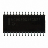
MC908QC16CDZE
Description
IC MCU 8BIT 16K FLASH 28-SOIC
Manufacturer
Freescale Semiconductor
Series
HC08r
Specifications of MC908QC16CDZE
Core Processor
HC08
Core Size
8-Bit
Speed
8MHz
Connectivity
SCI, SPI
Peripherals
LVD, POR, PWM
Number Of I /o
24
Program Memory Size
16KB (16K x 8)
Program Memory Type
FLASH
Ram Size
512 x 8
Voltage - Supply (vcc/vdd)
3 V ~ 5.5 V
Data Converters
A/D 10x10b
Oscillator Type
Internal
Operating Temperature
-40°C ~ 85°C
Package / Case
28-SOIC (7.5mm Width)
Processor Series
HC08QC
Core
HC08
Data Bus Width
8 bit
Data Ram Size
512 B
Interface Type
ESCI/SPI
Maximum Clock Frequency
8 MHz
Number Of Programmable I/os
26
Number Of Timers
6
Maximum Operating Temperature
+ 85 C
Mounting Style
SMD/SMT
Development Tools By Supplier
FSICEBASE, M68CBL05AE, DEMO908QB8, DEMO908QC16
Minimum Operating Temperature
- 40 C
On-chip Adc
10-ch x 10-bit
For Use With
DEMO908QC16 - BOARD DEMO FOR MC908QC16
Lead Free Status / RoHS Status
Lead free / RoHS Compliant
Eeprom Size
-
Lead Free Status / Rohs Status
Lead free / RoHS Compliant
Available stocks
Company
Part Number
Manufacturer
Quantity
Price
Company:

Part Number:
MC908QC16CDZE
Manufacturer:
FREESCALE
Quantity:
1 600
Part Number:
MC908QC16CDZE
Manufacturer:
FREESCALE
Quantity:
20 000


Oscillator Mode (OSC)
OSCOPT1:OSCOPT0 — OSC Option Bits
ICFS1:ICFS0 — Internal Clock Frequency Select Bits
ECFS1:ECFS0 — External Crystal Frequency Select Bits
ECGON — External Clock Generator On Bit
104
These read/write bits allow the user to change the clock source for the MCU. The default reset
condition has the bus clock being derived from the internal oscillator. See
Clock Switching
These read/write bits enable the frequency to be increased for applications requiring a faster bus clock
when running off the internal oscillator. The WAIT instruction has no effect on the oscillator logic.
BUSCLKX2 and BUSCLKX4 continue to drive to the SIM module.
These read/write bits enable the specific amplifier for the crystal frequency range. Refer to oscillator
characteristics table in the Electricals section for information on maximum external clock frequency
versus supply voltage.
This read/write bit enables the OSC1 pin as the clock input to the MCU, so that the switching process
can be initiated. This bit is cleared by reset. This bit is ignored in monitor mode with the internal
oscillator bypassed.
1 = External clock enabled
0 = External clock disabled
Reset:
Read:
Write:
OSCOPT1
ECFS1
ICFS1
Figure 10-4. Oscillator Status and Control Register (OSCSC)
for information on changing clock sources.
MC68HC908QC16 • MC68HC908QC8 • MC68HC908QC4 Data Sheet, Rev. 5
OSCOPT1
0
0
1
1
0
0
1
1
0
0
1
1
Bit 7
0
= Unimplemented
OSCOPT0
OSCOPT0
ECFS0
ICFS0
6
0
0
1
0
1
0
1
0
1
0
1
0
1
ICFS1
4.0 MHz — default reset condition
8.0 MHz
12.8 MHz
25.6 MHz
8 MHz – 32 MHz
1 MHz – 8 MHz
32 kHz – 100 kHz
Reserved
Internal oscillator (frequency selected using ICFSx bits)
External oscillator clock
External RC
External crystal (range selected using ECFSx bits)
5
0
ICFS0
4
0
External Crystal Frequency
Internal Clock Frequency
Oscillator Modes
ECFS1
3
0
ECFS0
2
0
ECGON
10.3.2.2 Internal to External
1
0
Freescale Semiconductor
ECGST
Bit 0
0
Related parts for MC908QC16CDZE
Image
Part Number
Description
Manufacturer
Datasheet
Request
R

Part Number:
Description:
Manufacturer:
Freescale Semiconductor, Inc
Datasheet:
Part Number:
Description:
Manufacturer:
Freescale Semiconductor, Inc
Datasheet:
Part Number:
Description:
Manufacturer:
Freescale Semiconductor, Inc
Datasheet:
Part Number:
Description:
Manufacturer:
Freescale Semiconductor, Inc
Datasheet:
Part Number:
Description:
Manufacturer:
Freescale Semiconductor, Inc
Datasheet:
Part Number:
Description:
Manufacturer:
Freescale Semiconductor, Inc
Datasheet:
Part Number:
Description:
Manufacturer:
Freescale Semiconductor, Inc
Datasheet:
Part Number:
Description:
Manufacturer:
Freescale Semiconductor, Inc
Datasheet:
Part Number:
Description:
Manufacturer:
Freescale Semiconductor, Inc
Datasheet:
Part Number:
Description:
Manufacturer:
Freescale Semiconductor, Inc
Datasheet:
Part Number:
Description:
Manufacturer:
Freescale Semiconductor, Inc
Datasheet:
Part Number:
Description:
Manufacturer:
Freescale Semiconductor, Inc
Datasheet:
Part Number:
Description:
Manufacturer:
Freescale Semiconductor, Inc
Datasheet:
Part Number:
Description:
Manufacturer:
Freescale Semiconductor, Inc
Datasheet:
Part Number:
Description:
Manufacturer:
Freescale Semiconductor, Inc
Datasheet: