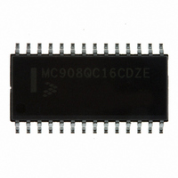
MC908QC16CDZE Freescale Semiconductor, MC908QC16CDZE Datasheet - Page 185

MC908QC16CDZE
Manufacturer Part Number
MC908QC16CDZE
Description
IC MCU 8BIT 16K FLASH 28-SOIC
Manufacturer
Freescale Semiconductor
Series
HC08r
Specifications of MC908QC16CDZE
Core Processor
HC08
Core Size
8-Bit
Speed
8MHz
Connectivity
SCI, SPI
Peripherals
LVD, POR, PWM
Number Of I /o
24
Program Memory Size
16KB (16K x 8)
Program Memory Type
FLASH
Ram Size
512 x 8
Voltage - Supply (vcc/vdd)
3 V ~ 5.5 V
Data Converters
A/D 10x10b
Oscillator Type
Internal
Operating Temperature
-40°C ~ 85°C
Package / Case
28-SOIC (7.5mm Width)
Processor Series
HC08QC
Core
HC08
Data Bus Width
8 bit
Data Ram Size
512 B
Interface Type
ESCI/SPI
Maximum Clock Frequency
8 MHz
Number Of Programmable I/os
26
Number Of Timers
6
Maximum Operating Temperature
+ 85 C
Mounting Style
SMD/SMT
Development Tools By Supplier
FSICEBASE, M68CBL05AE, DEMO908QB8, DEMO908QC16
Minimum Operating Temperature
- 40 C
On-chip Adc
10-ch x 10-bit
For Use With
DEMO908QC16 - BOARD DEMO FOR MC908QC16
Lead Free Status / RoHS Status
Lead free / RoHS Compliant
Eeprom Size
-
Lead Free Status / Rohs Status
Lead free / RoHS Compliant
Available stocks
Company
Part Number
Manufacturer
Quantity
Price
Company:
Part Number:
MC908QC16CDZE
Manufacturer:
FREESCALE
Quantity:
1 600
Part Number:
MC908QC16CDZE
Manufacturer:
FREESCALE
Quantity:
20 000
- Current page: 185 of 274
- Download datasheet (4Mb)
SPRIE — SPI Receiver Interrupt Enable Bit
SPMSTR — SPI Master Bit
CPOL — Clock Polarity Bit
CPHA — Clock Phase Bit
SPWOM — SPI Wired-OR Mode Bit
SPE — SPI Enable
SPTIE— SPI Transmit Interrupt Enable
Freescale Semiconductor
This read/write bit enables interrupt requests generated by the SPRF bit. The SPRF bit is set when a
byte transfers from the shift register to the receive data register.
This read/write bit selects master mode operation or slave mode operation.
This read/write bit determines the logic state of the SPSCK pin between transmissions. (See
Figure 15-4
identical CPOL values.
This read/write bit controls the timing relationship between the serial clock and SPI data. (See
Figure 15-4
identical CPHA values. When CPHA = 0, the SS pin of the slave SPI module must be high between
bytes. (See
This read/write bit configures pins SPSCK, MOSI, and MISO so that these pins become open-drain
outputs.
This read/write bit enables the SPI module. Clearing SPE causes a partial reset of the SPI. (See
Resetting the
This read/write bit enables interrupt requests generated by the SPTE bit. SPTE is set when a byte
transfers from the transmit data register to the shift register.
1 = SPRF interrupt requests enabled
0 = SPRF interrupt requests disabled
1 = Master mode
0 = Slave mode
1 = Wired-OR SPSCK, MOSI, and MISO pins
0 = Normal push-pull SPSCK, MOSI, and MISO pins
1 = SPI module enabled
0 = SPI module disabled
1 = SPTE interrupt requests enabled
0 = SPTE interrupt requests disabled
Reset:
Read:
Write:
Figure
and
and
SPI.)
Figure
Figure
MC68HC908QC16 • MC68HC908QC8 • MC68HC908QC4 Data Sheet, Rev. 5
SPRIE
15-12.)
Bit 7
R
0
15-6.) To transmit data between SPI modules, the SPI modules must have
15-6.) To transmit data between SPI modules, the SPI modules must have
= Reserved
Figure 15-13. SPI Control Register (SPCR)
R
6
0
SPMSTR
5
1
CPOL
4
0
CPHA
3
1
SPWOM
2
0
SPE
1
0
SPTIE
Bit 0
0
Registers
15.3.5
185
Related parts for MC908QC16CDZE
Image
Part Number
Description
Manufacturer
Datasheet
Request
R
Part Number:
Description:
Manufacturer:
Freescale Semiconductor, Inc
Datasheet:
Part Number:
Description:
Manufacturer:
Freescale Semiconductor, Inc
Datasheet:
Part Number:
Description:
Manufacturer:
Freescale Semiconductor, Inc
Datasheet:
Part Number:
Description:
Manufacturer:
Freescale Semiconductor, Inc
Datasheet:
Part Number:
Description:
Manufacturer:
Freescale Semiconductor, Inc
Datasheet:
Part Number:
Description:
Manufacturer:
Freescale Semiconductor, Inc
Datasheet:
Part Number:
Description:
Manufacturer:
Freescale Semiconductor, Inc
Datasheet:
Part Number:
Description:
Manufacturer:
Freescale Semiconductor, Inc
Datasheet:
Part Number:
Description:
Manufacturer:
Freescale Semiconductor, Inc
Datasheet:
Part Number:
Description:
Manufacturer:
Freescale Semiconductor, Inc
Datasheet:
Part Number:
Description:
Manufacturer:
Freescale Semiconductor, Inc
Datasheet:
Part Number:
Description:
Manufacturer:
Freescale Semiconductor, Inc
Datasheet:
Part Number:
Description:
Manufacturer:
Freescale Semiconductor, Inc
Datasheet:
Part Number:
Description:
Manufacturer:
Freescale Semiconductor, Inc
Datasheet:
Part Number:
Description:
Manufacturer:
Freescale Semiconductor, Inc
Datasheet:


