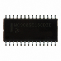
MC908QC16CDZE Freescale Semiconductor, MC908QC16CDZE Datasheet - Page 228

MC908QC16CDZE
Manufacturer Part Number
MC908QC16CDZE
Description
IC MCU 8BIT 16K FLASH 28-SOIC
Manufacturer
Freescale Semiconductor
Series
HC08r
Specifications of MC908QC16CDZE
Core Processor
HC08
Core Size
8-Bit
Speed
8MHz
Connectivity
SCI, SPI
Peripherals
LVD, POR, PWM
Number Of I /o
24
Program Memory Size
16KB (16K x 8)
Program Memory Type
FLASH
Ram Size
512 x 8
Voltage - Supply (vcc/vdd)
3 V ~ 5.5 V
Data Converters
A/D 10x10b
Oscillator Type
Internal
Operating Temperature
-40°C ~ 85°C
Package / Case
28-SOIC (7.5mm Width)
Processor Series
HC08QC
Core
HC08
Data Bus Width
8 bit
Data Ram Size
512 B
Interface Type
ESCI/SPI
Maximum Clock Frequency
8 MHz
Number Of Programmable I/os
26
Number Of Timers
6
Maximum Operating Temperature
+ 85 C
Mounting Style
SMD/SMT
Development Tools By Supplier
FSICEBASE, M68CBL05AE, DEMO908QB8, DEMO908QC16
Minimum Operating Temperature
- 40 C
On-chip Adc
10-ch x 10-bit
For Use With
DEMO908QC16 - BOARD DEMO FOR MC908QC16
Lead Free Status / RoHS Status
Lead free / RoHS Compliant
Eeprom Size
-
Lead Free Status / Rohs Status
Lead free / RoHS Compliant
Available stocks
Company
Part Number
Manufacturer
Quantity
Price
Company:
Part Number:
MC908QC16CDZE
Manufacturer:
FREESCALE
Quantity:
1 600
Part Number:
MC908QC16CDZE
Manufacturer:
FREESCALE
Quantity:
20 000
- Current page: 228 of 274
- Download datasheet (4Mb)
Development Support
The rising edge of the internal RST signal latches the monitor mode. Once monitor mode is latched, the
values on PTA1 and PTA4 pins can be changed.
Once out of reset, the MCU waits for the host to send eight security bytes (see
security bytes, the MCU sends a break signal (10 consecutive 0s) to the host, indicating that it is ready to
receive a command.
18.3.1.1 Normal Monitor Mode
RST and OSC1 functions will be active on the PTA3 and PTA5 pins respectively as long as V
applied to the IRQ pin. If the IRQ pin is lowered (no longer V
monitor mode, but the pin functions will be determined by the settings in the configuration registers (see
Chapter 4 Configuration Registers (CONFIG1 and
lowered, the BIH and BIL instructions will read the IRQ pin state only if IRQEN is set in the CONFIG2
register.
228
Function
[Pin No.]
MON08
Monitor
Monitor
Normal
Forced
Mode
1. PTA0 must have a pullup resistor to V
2. Communication speed in the table is an example to obtain a baud rate of 9600. Baud rate using external oscillator is bus
3. External clock is a 9.8304 MHz oscillator on OSC1.
4. X = don’t care
5. MON08 pin refers to P&E Microcomputer Systems’ MON08-Cyclone 2 by 8-pin connector.
User
frequency / 256 and baud rate using internal oscillator is bus frequency / 335.
(PTA2)
V
V
V
IRQ
V
[6]
TST
TST
X
DD
SS
(PTA3)
RST
RST
V
[4]
X
X
X
DD
MC68HC908QC16 • MC68HC908QC8 • MC68HC908QC4 Data Sheet, Rev. 5
Table 18-1. Monitor Mode Signal Requirements and Options
Vector
(blank)
(blank)
$FFFF
$FFFF
$FFFF
Reset
Not
—
X
Communi-
cation
Serial
PTA0
COM
[8]
X
1
1
1
DD
OSC1
V
NC
NC
NC
NC
NC
NC
in monitor mode.
DD
PTA1 PTA4
MOD
[12]
Selection
11
13
15
X
X
X
1
0
1
3
5
7
9
Mode
MOD
[10]
10
12
14
16
X
X
X
0
1
2
4
6
8
CONFIG2)) when V
Disabled
Disabled
Disabled
Enabled
GND
RST
IRQ
PTA0
PTA4
PTA1
NC
NC
COP
—
TST
External
9.8304
9.8304
) then the chip will still be operating in
Clock
OSC1
MHz
MHz
[13]
X
X
Communication
TST
Frequency
(Trimmed)
Speed
3.2 MHz
2.4576
2.4576
MHz
MHz
was lowered. With V
Bus
—
X
18.3.2
Freescale Semiconductor
Baud
Rate
9600
9600
9600
—
X
Security). After the
Provide external
clock at OSC1.
Provide external
clock at OSC1.
Internal clock is
active.
Comments
TST
TST
is
Related parts for MC908QC16CDZE
Image
Part Number
Description
Manufacturer
Datasheet
Request
R
Part Number:
Description:
Manufacturer:
Freescale Semiconductor, Inc
Datasheet:
Part Number:
Description:
Manufacturer:
Freescale Semiconductor, Inc
Datasheet:
Part Number:
Description:
Manufacturer:
Freescale Semiconductor, Inc
Datasheet:
Part Number:
Description:
Manufacturer:
Freescale Semiconductor, Inc
Datasheet:
Part Number:
Description:
Manufacturer:
Freescale Semiconductor, Inc
Datasheet:
Part Number:
Description:
Manufacturer:
Freescale Semiconductor, Inc
Datasheet:
Part Number:
Description:
Manufacturer:
Freescale Semiconductor, Inc
Datasheet:
Part Number:
Description:
Manufacturer:
Freescale Semiconductor, Inc
Datasheet:
Part Number:
Description:
Manufacturer:
Freescale Semiconductor, Inc
Datasheet:
Part Number:
Description:
Manufacturer:
Freescale Semiconductor, Inc
Datasheet:
Part Number:
Description:
Manufacturer:
Freescale Semiconductor, Inc
Datasheet:
Part Number:
Description:
Manufacturer:
Freescale Semiconductor, Inc
Datasheet:
Part Number:
Description:
Manufacturer:
Freescale Semiconductor, Inc
Datasheet:
Part Number:
Description:
Manufacturer:
Freescale Semiconductor, Inc
Datasheet:
Part Number:
Description:
Manufacturer:
Freescale Semiconductor, Inc
Datasheet:


