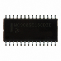
MC908QC16CDZE Freescale Semiconductor, MC908QC16CDZE Datasheet - Page 212

MC908QC16CDZE
Manufacturer Part Number
MC908QC16CDZE
Description
IC MCU 8BIT 16K FLASH 28-SOIC
Manufacturer
Freescale Semiconductor
Series
HC08r
Specifications of MC908QC16CDZE
Core Processor
HC08
Core Size
8-Bit
Speed
8MHz
Connectivity
SCI, SPI
Peripherals
LVD, POR, PWM
Number Of I /o
24
Program Memory Size
16KB (16K x 8)
Program Memory Type
FLASH
Ram Size
512 x 8
Voltage - Supply (vcc/vdd)
3 V ~ 5.5 V
Data Converters
A/D 10x10b
Oscillator Type
Internal
Operating Temperature
-40°C ~ 85°C
Package / Case
28-SOIC (7.5mm Width)
Processor Series
HC08QC
Core
HC08
Data Bus Width
8 bit
Data Ram Size
512 B
Interface Type
ESCI/SPI
Maximum Clock Frequency
8 MHz
Number Of Programmable I/os
26
Number Of Timers
6
Maximum Operating Temperature
+ 85 C
Mounting Style
SMD/SMT
Development Tools By Supplier
FSICEBASE, M68CBL05AE, DEMO908QB8, DEMO908QC16
Minimum Operating Temperature
- 40 C
On-chip Adc
10-ch x 10-bit
For Use With
DEMO908QC16 - BOARD DEMO FOR MC908QC16
Lead Free Status / RoHS Status
Lead free / RoHS Compliant
Eeprom Size
-
Lead Free Status / Rohs Status
Lead free / RoHS Compliant
Available stocks
Company
Part Number
Manufacturer
Quantity
Price
Company:
Part Number:
MC908QC16CDZE
Manufacturer:
FREESCALE
Quantity:
1 600
Part Number:
MC908QC16CDZE
Manufacturer:
FREESCALE
Quantity:
20 000
- Current page: 212 of 274
- Download datasheet (4Mb)
Timer Interface Module (TIM2)
To allow software to clear status bits during a break interrupt, write a 1 to BCFE. If a status bit is cleared
during the break state, it remains cleared when the MCU exits the break state.
To protect status bits during the break state, write a 0 to BCFE. With BCFE cleared (its default state),
software can read and write registers during the break state without affecting status bits. Some status bits
have a two-step read/write clearing procedure. If software does the first step on such a bit before the
break, the bit cannot change during the break state as long as BCFE is cleared. After the break, doing
the second step clears the status bit.
17.7 I/O Signals
The TIM2 module can share its pins with the general-purpose I/O pins. See
that are shared.
17.7.1 TIM2 Channel I/O Pins (T2CH1:T2CH0)
Each channel I/O pin is programmable independently as an input capture pin or an output compare pin.
T
17.7.2 TIM2 Clock Pin (T2CLK)
T2CLK is an external clock input that can be the clock source for the counter instead of the prescaled
internal bus clock. Select the T2CLK input by writing 1s to the three prescaler select bits, PS[2:0]. The
minimum T2CLK pulse width is specified in the Timer Interface Module Characteristics table in the
Electricals section. The maximum T2CLK frequency is the least of 4 MHz or bus
frequency ÷ 2.
17.8 Registers
The following registers control and monitor operation of the TIM2:
17.8.1 TIM2 Status and Control Register
The TIM2 status and control register (T2SC) does the following:
212
2
CH0
•
•
•
•
•
•
•
•
•
•
TIM2 status and control register (T2SC)
TIM2 control registers (T2CNTH:T2CNTL)
TIM2 counter modulo registers (T2MODH:T2MODL)
TIM2 channel status and control registers (T2SC0 and T2SC1)
TIM2 channel registers (T2CH0H:T2CH0L and T2CH1H:T2CH1L)
Enables TIM2 overflow interrupts
Flags TIM2 overflows
Stops the counter
Resets the counter
Prescales the counter clock
can be configured as buffered output compare or buffered PWM pin.
MC68HC908QC16 • MC68HC908QC8 • MC68HC908QC4 Data Sheet, Rev. 5
Figure 17-1
Freescale Semiconductor
for the port pins
Related parts for MC908QC16CDZE
Image
Part Number
Description
Manufacturer
Datasheet
Request
R
Part Number:
Description:
Manufacturer:
Freescale Semiconductor, Inc
Datasheet:
Part Number:
Description:
Manufacturer:
Freescale Semiconductor, Inc
Datasheet:
Part Number:
Description:
Manufacturer:
Freescale Semiconductor, Inc
Datasheet:
Part Number:
Description:
Manufacturer:
Freescale Semiconductor, Inc
Datasheet:
Part Number:
Description:
Manufacturer:
Freescale Semiconductor, Inc
Datasheet:
Part Number:
Description:
Manufacturer:
Freescale Semiconductor, Inc
Datasheet:
Part Number:
Description:
Manufacturer:
Freescale Semiconductor, Inc
Datasheet:
Part Number:
Description:
Manufacturer:
Freescale Semiconductor, Inc
Datasheet:
Part Number:
Description:
Manufacturer:
Freescale Semiconductor, Inc
Datasheet:
Part Number:
Description:
Manufacturer:
Freescale Semiconductor, Inc
Datasheet:
Part Number:
Description:
Manufacturer:
Freescale Semiconductor, Inc
Datasheet:
Part Number:
Description:
Manufacturer:
Freescale Semiconductor, Inc
Datasheet:
Part Number:
Description:
Manufacturer:
Freescale Semiconductor, Inc
Datasheet:
Part Number:
Description:
Manufacturer:
Freescale Semiconductor, Inc
Datasheet:
Part Number:
Description:
Manufacturer:
Freescale Semiconductor, Inc
Datasheet:


