MC908QC16CDZE Freescale Semiconductor, MC908QC16CDZE Datasheet - Page 52
MC908QC16CDZE
Manufacturer Part Number
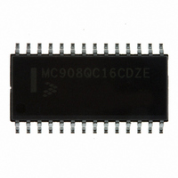
MC908QC16CDZE
Description
IC MCU 8BIT 16K FLASH 28-SOIC
Manufacturer
Freescale Semiconductor
Series
HC08r
Specifications of MC908QC16CDZE
Core Processor
HC08
Core Size
8-Bit
Speed
8MHz
Connectivity
SCI, SPI
Peripherals
LVD, POR, PWM
Number Of I /o
24
Program Memory Size
16KB (16K x 8)
Program Memory Type
FLASH
Ram Size
512 x 8
Voltage - Supply (vcc/vdd)
3 V ~ 5.5 V
Data Converters
A/D 10x10b
Oscillator Type
Internal
Operating Temperature
-40°C ~ 85°C
Package / Case
28-SOIC (7.5mm Width)
Processor Series
HC08QC
Core
HC08
Data Bus Width
8 bit
Data Ram Size
512 B
Interface Type
ESCI/SPI
Maximum Clock Frequency
8 MHz
Number Of Programmable I/os
26
Number Of Timers
6
Maximum Operating Temperature
+ 85 C
Mounting Style
SMD/SMT
Development Tools By Supplier
FSICEBASE, M68CBL05AE, DEMO908QB8, DEMO908QC16
Minimum Operating Temperature
- 40 C
On-chip Adc
10-ch x 10-bit
For Use With
DEMO908QC16 - BOARD DEMO FOR MC908QC16
Lead Free Status / RoHS Status
Lead free / RoHS Compliant
Eeprom Size
-
Lead Free Status / Rohs Status
Lead free / RoHS Compliant
Available stocks
Company
Part Number
Manufacturer
Quantity
Price
Company:

Part Number:
MC908QC16CDZE
Manufacturer:
FREESCALE
Quantity:
1 600
Part Number:
MC908QC16CDZE
Manufacturer:
FREESCALE
Quantity:
20 000


Analog-to-Digital Converter (ADC10) Module
3.4 Interrupts
When AIEN is set, the ADC10 is capable of generating an interrupt request after each conversion. An
interrupt request is generated when the conversion completes (indicated by COCO being set). COCO will
set at the end of a conversion regardless of the state of AIEN.
3.5 Low-Power Modes
The WAIT and STOP instructions put the MCU in low power-consumption standby modes.
3.5.1 Wait Mode
The ADC10 will continue the conversion process and will generate an interrupt request following a
conversion if AIEN is set. If the ADC10 is not required in wait mode, power down the ADC by setting the
channel select bits (ADCH[4:0]) to all 1s to enter a low power state before executing the WAIT instruction.
3.5.2 Stop Mode
If ACLKEN is clear, executing a STOP instruction will abort the current conversion and place the ADC10
in a low-power state. Upon return from stop mode, a write to ADSCR is required to resume conversions,
and the result stored in ADRH and ADRL will represent the last completed conversion until the new
conversion completes.
If ACLKEN is set, the ADC10 continues normal operation during stop mode. The ADC10 will continue the
conversion process and will generate an interrupt following a conversion if AIEN is set. If the ADC10 is
not required to bring the MCU out of stop mode, ensure that the ADC10 is not in continuous conversion
mode by clearing ADCO in the ADC10 status and control register before executing the STOP instruction.
In single conversion mode the ADC10 automatically enters a low-power state when the conversion is
complete. It is not necessary to set the channel select bits (ADCH[4:0]) to all 1s to enter a low-power state.
If ACLKEN is set, a conversion can be initiated while in stop using the external hardware trigger
ADEXTCO when in external convert mode. The ADC10 will operate in a low-power mode until the trigger
is asserted, at which point it will perform a conversion and assert the interrupt when complete (if AIEN is
set).
3.6 ADC10 During Break Interrupts
The system integration module (SIM) controls whether status bits in other modules can be cleared during
the break state. BCFE in the break flag control register (BFCR) enables software to clear status bits
during the break state. See BFCR in the SIM section of this data
sheet.
To allow software to clear status bits during a break interrupt, write a 1 to BCFE. If a status bit is cleared
during the break state, it remains cleared when the MCU exits the break state.
To protect status bits during the break state, write a 0 to BCFE. With BCFE cleared (its default state),
software can read and write registers during the break state without affecting status bits. Some status bits
have a two-step read/write clearing procedure. If software does the first step on such a bit before the
break, the bit cannot change during the break state as long as BCFE is cleared. After the break, doing
the second step clears the status bit.
MC68HC908QC16 • MC68HC908QC8 • MC68HC908QC4 Data Sheet, Rev. 5
52
Freescale Semiconductor
Related parts for MC908QC16CDZE
Image
Part Number
Description
Manufacturer
Datasheet
Request
R

Part Number:
Description:
Manufacturer:
Freescale Semiconductor, Inc
Datasheet:
Part Number:
Description:
Manufacturer:
Freescale Semiconductor, Inc
Datasheet:
Part Number:
Description:
Manufacturer:
Freescale Semiconductor, Inc
Datasheet:
Part Number:
Description:
Manufacturer:
Freescale Semiconductor, Inc
Datasheet:
Part Number:
Description:
Manufacturer:
Freescale Semiconductor, Inc
Datasheet:
Part Number:
Description:
Manufacturer:
Freescale Semiconductor, Inc
Datasheet:
Part Number:
Description:
Manufacturer:
Freescale Semiconductor, Inc
Datasheet:
Part Number:
Description:
Manufacturer:
Freescale Semiconductor, Inc
Datasheet:
Part Number:
Description:
Manufacturer:
Freescale Semiconductor, Inc
Datasheet:
Part Number:
Description:
Manufacturer:
Freescale Semiconductor, Inc
Datasheet:
Part Number:
Description:
Manufacturer:
Freescale Semiconductor, Inc
Datasheet:
Part Number:
Description:
Manufacturer:
Freescale Semiconductor, Inc
Datasheet:
Part Number:
Description:
Manufacturer:
Freescale Semiconductor, Inc
Datasheet:
Part Number:
Description:
Manufacturer:
Freescale Semiconductor, Inc
Datasheet:
Part Number:
Description:
Manufacturer:
Freescale Semiconductor, Inc
Datasheet: