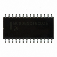
MC908QC16CDZE Freescale Semiconductor, MC908QC16CDZE Datasheet - Page 140

MC908QC16CDZE
Manufacturer Part Number
MC908QC16CDZE
Description
IC MCU 8BIT 16K FLASH 28-SOIC
Manufacturer
Freescale Semiconductor
Series
HC08r
Specifications of MC908QC16CDZE
Core Processor
HC08
Core Size
8-Bit
Speed
8MHz
Connectivity
SCI, SPI
Peripherals
LVD, POR, PWM
Number Of I /o
24
Program Memory Size
16KB (16K x 8)
Program Memory Type
FLASH
Ram Size
512 x 8
Voltage - Supply (vcc/vdd)
3 V ~ 5.5 V
Data Converters
A/D 10x10b
Oscillator Type
Internal
Operating Temperature
-40°C ~ 85°C
Package / Case
28-SOIC (7.5mm Width)
Processor Series
HC08QC
Core
HC08
Data Bus Width
8 bit
Data Ram Size
512 B
Interface Type
ESCI/SPI
Maximum Clock Frequency
8 MHz
Number Of Programmable I/os
26
Number Of Timers
6
Maximum Operating Temperature
+ 85 C
Mounting Style
SMD/SMT
Development Tools By Supplier
FSICEBASE, M68CBL05AE, DEMO908QB8, DEMO908QC16
Minimum Operating Temperature
- 40 C
On-chip Adc
10-ch x 10-bit
For Use With
DEMO908QC16 - BOARD DEMO FOR MC908QC16
Lead Free Status / RoHS Status
Lead free / RoHS Compliant
Eeprom Size
-
Lead Free Status / Rohs Status
Lead free / RoHS Compliant
Available stocks
Company
Part Number
Manufacturer
Quantity
Price
Company:
Part Number:
MC908QC16CDZE
Manufacturer:
FREESCALE
Quantity:
1 600
Part Number:
MC908QC16CDZE
Manufacturer:
FREESCALE
Quantity:
20 000
- Current page: 140 of 274
- Download datasheet (4Mb)
Enhanced Serial Communications Interface (ESCI) Module
13.8.3 ESCI Control Register 3
ESCI control register 3 (SCC3):
R8 — Received Bit 8
T8 — Transmitted Bit 8
ORIE — Receiver Overrun Interrupt Enable Bit
NEIE — Receiver Noise Error Interrupt Enable Bit
FEIE — Receiver Framing Error Interrupt Enable Bit
PEIE — Receiver Parity Error Interrupt Enable Bit
140
•
•
When the ESCI is receiving 9-bit characters, R8 is the read-only ninth bit (bit 8) of the received
character. R8 is received at the same time that the SCDR receives the other 8 bits.
When the ESCI is receiving 8-bit characters, R8 is a copy of the eighth bit (bit 7).
When the ESCI is transmitting 9-bit characters, T8 is the read/write ninth bit (bit 8) of the transmitted
character. T8 is loaded into the transmit shift register at the same time that the SCDR is loaded into
the transmit shift register.
This read/write bit enables ESCI error interrupt requests generated by the receiver overrun bit, OR.
This read/write bit enables ESCI error interrupt requests generated by the noise error bit, NE.
This read/write bit enables ESCI error interrupt requests generated by the framing error bit, FE.
This read/write bit enables ESCI receiver interrupt requests generated by the parity error bit, PE.
1 = ESCI error interrupt requests from OR bit enabled
0 = ESCI error interrupt requests from OR bit disabled
1 = ESCI error interrupt requests from NE bit enabled
0 = ESCI error interrupt requests from NE bit disabled
1 = ESCI error interrupt requests from FE bit enabled
0 = ESCI error interrupt requests from FE bit disabled
1 = ESCI error interrupt requests from PE bit enabled
0 = ESCI error interrupt requests from PE bit disabled
Stores the ninth ESCI data bit received and the ninth ESCI data bit to be transmitted.
Enables these interrupts:
–
–
–
–
Receiver overrun
Noise error
Framing error
Parity error
Reset:
Read:
Write:
MC68HC908QC16 • MC68HC908QC8 • MC68HC908QC4 Data Sheet, Rev. 5
Bit 7
R8
U
Figure 13-11. ESCI Control Register 3 (SCC3)
= Unimplemented
T8
6
0
R
5
0
R
R
4
0
= Reserved
ORIE
3
0
NEIE
U = Unaffected
2
0
FEIE
1
0
Freescale Semiconductor
PEIE
Bit 0
0
Related parts for MC908QC16CDZE
Image
Part Number
Description
Manufacturer
Datasheet
Request
R
Part Number:
Description:
Manufacturer:
Freescale Semiconductor, Inc
Datasheet:
Part Number:
Description:
Manufacturer:
Freescale Semiconductor, Inc
Datasheet:
Part Number:
Description:
Manufacturer:
Freescale Semiconductor, Inc
Datasheet:
Part Number:
Description:
Manufacturer:
Freescale Semiconductor, Inc
Datasheet:
Part Number:
Description:
Manufacturer:
Freescale Semiconductor, Inc
Datasheet:
Part Number:
Description:
Manufacturer:
Freescale Semiconductor, Inc
Datasheet:
Part Number:
Description:
Manufacturer:
Freescale Semiconductor, Inc
Datasheet:
Part Number:
Description:
Manufacturer:
Freescale Semiconductor, Inc
Datasheet:
Part Number:
Description:
Manufacturer:
Freescale Semiconductor, Inc
Datasheet:
Part Number:
Description:
Manufacturer:
Freescale Semiconductor, Inc
Datasheet:
Part Number:
Description:
Manufacturer:
Freescale Semiconductor, Inc
Datasheet:
Part Number:
Description:
Manufacturer:
Freescale Semiconductor, Inc
Datasheet:
Part Number:
Description:
Manufacturer:
Freescale Semiconductor, Inc
Datasheet:
Part Number:
Description:
Manufacturer:
Freescale Semiconductor, Inc
Datasheet:
Part Number:
Description:
Manufacturer:
Freescale Semiconductor, Inc
Datasheet:


