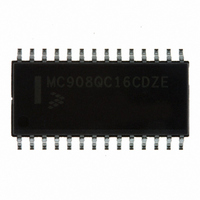
MC908QC16CDZE Freescale Semiconductor, MC908QC16CDZE Datasheet - Page 166

MC908QC16CDZE
Manufacturer Part Number
MC908QC16CDZE
Description
IC MCU 8BIT 16K FLASH 28-SOIC
Manufacturer
Freescale Semiconductor
Series
HC08r
Specifications of MC908QC16CDZE
Core Processor
HC08
Core Size
8-Bit
Speed
8MHz
Connectivity
SCI, SPI
Peripherals
LVD, POR, PWM
Number Of I /o
24
Program Memory Size
16KB (16K x 8)
Program Memory Type
FLASH
Ram Size
512 x 8
Voltage - Supply (vcc/vdd)
3 V ~ 5.5 V
Data Converters
A/D 10x10b
Oscillator Type
Internal
Operating Temperature
-40°C ~ 85°C
Package / Case
28-SOIC (7.5mm Width)
Processor Series
HC08QC
Core
HC08
Data Bus Width
8 bit
Data Ram Size
512 B
Interface Type
ESCI/SPI
Maximum Clock Frequency
8 MHz
Number Of Programmable I/os
26
Number Of Timers
6
Maximum Operating Temperature
+ 85 C
Mounting Style
SMD/SMT
Development Tools By Supplier
FSICEBASE, M68CBL05AE, DEMO908QB8, DEMO908QC16
Minimum Operating Temperature
- 40 C
On-chip Adc
10-ch x 10-bit
For Use With
DEMO908QC16 - BOARD DEMO FOR MC908QC16
Lead Free Status / RoHS Status
Lead free / RoHS Compliant
Eeprom Size
-
Lead Free Status / Rohs Status
Lead free / RoHS Compliant
Available stocks
Company
Part Number
Manufacturer
Quantity
Price
Company:
Part Number:
MC908QC16CDZE
Manufacturer:
FREESCALE
Quantity:
1 600
Part Number:
MC908QC16CDZE
Manufacturer:
FREESCALE
Quantity:
20 000
- Current page: 166 of 274
- Download datasheet (4Mb)
System Integration Module (SIM)
The SIM counter is held in reset from the execution of the STOP instruction until the beginning of stop
recovery. It is then used to time the recovery period.
Figure 14-18
14.8 SIM Registers
The SIM has three memory mapped registers.
166
ADDRESS BUS
INTERRUPT
BUSCLKX4
ADDRESS BUS
NOTE: Previous data can be operand data or the STOP opcode, depending on the last instruction.
shows the stop mode recovery time from interrupt or break
To minimize stop current, all pins configured as inputs should be driven to
a logic 1 or logic 0.
DATA BUS
CPUSTOP
MC68HC908QC16 • MC68HC908QC8 • MC68HC908QC4 Data Sheet, Rev. 5
R/W
Figure 14-18. Stop Mode Recovery from Interrupt
Address
STOP ADDR
$FE00
$FE01
$FE03
STOP +1
Figure 14-17. Stop Mode Entry Timing
PREVIOUS DATA
Table 14-4. SIM Registers
STOP ADDR + 1
Register
SRSR
BFCR
BSR
Table 14-4
STOP + 2
NOTE
STOP RECOVERY PERIOD
NEXT OPCODE
Figure 14-17
STOP + 2
shows the mapping of these registers.
SAME
Access Mode
shows stop mode entry timing and
User
User
User
SP
SAME
SP – 1
SAME
SAME
Freescale Semiconductor
SP – 2
SP – 3
Related parts for MC908QC16CDZE
Image
Part Number
Description
Manufacturer
Datasheet
Request
R
Part Number:
Description:
Manufacturer:
Freescale Semiconductor, Inc
Datasheet:
Part Number:
Description:
Manufacturer:
Freescale Semiconductor, Inc
Datasheet:
Part Number:
Description:
Manufacturer:
Freescale Semiconductor, Inc
Datasheet:
Part Number:
Description:
Manufacturer:
Freescale Semiconductor, Inc
Datasheet:
Part Number:
Description:
Manufacturer:
Freescale Semiconductor, Inc
Datasheet:
Part Number:
Description:
Manufacturer:
Freescale Semiconductor, Inc
Datasheet:
Part Number:
Description:
Manufacturer:
Freescale Semiconductor, Inc
Datasheet:
Part Number:
Description:
Manufacturer:
Freescale Semiconductor, Inc
Datasheet:
Part Number:
Description:
Manufacturer:
Freescale Semiconductor, Inc
Datasheet:
Part Number:
Description:
Manufacturer:
Freescale Semiconductor, Inc
Datasheet:
Part Number:
Description:
Manufacturer:
Freescale Semiconductor, Inc
Datasheet:
Part Number:
Description:
Manufacturer:
Freescale Semiconductor, Inc
Datasheet:
Part Number:
Description:
Manufacturer:
Freescale Semiconductor, Inc
Datasheet:
Part Number:
Description:
Manufacturer:
Freescale Semiconductor, Inc
Datasheet:
Part Number:
Description:
Manufacturer:
Freescale Semiconductor, Inc
Datasheet:


