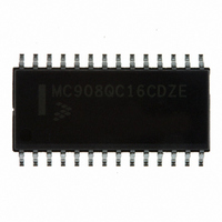
MC908QC16CDZE Freescale Semiconductor, MC908QC16CDZE Datasheet - Page 53

MC908QC16CDZE
Manufacturer Part Number
MC908QC16CDZE
Description
IC MCU 8BIT 16K FLASH 28-SOIC
Manufacturer
Freescale Semiconductor
Series
HC08r
Specifications of MC908QC16CDZE
Core Processor
HC08
Core Size
8-Bit
Speed
8MHz
Connectivity
SCI, SPI
Peripherals
LVD, POR, PWM
Number Of I /o
24
Program Memory Size
16KB (16K x 8)
Program Memory Type
FLASH
Ram Size
512 x 8
Voltage - Supply (vcc/vdd)
3 V ~ 5.5 V
Data Converters
A/D 10x10b
Oscillator Type
Internal
Operating Temperature
-40°C ~ 85°C
Package / Case
28-SOIC (7.5mm Width)
Processor Series
HC08QC
Core
HC08
Data Bus Width
8 bit
Data Ram Size
512 B
Interface Type
ESCI/SPI
Maximum Clock Frequency
8 MHz
Number Of Programmable I/os
26
Number Of Timers
6
Maximum Operating Temperature
+ 85 C
Mounting Style
SMD/SMT
Development Tools By Supplier
FSICEBASE, M68CBL05AE, DEMO908QB8, DEMO908QC16
Minimum Operating Temperature
- 40 C
On-chip Adc
10-ch x 10-bit
For Use With
DEMO908QC16 - BOARD DEMO FOR MC908QC16
Lead Free Status / RoHS Status
Lead free / RoHS Compliant
Eeprom Size
-
Lead Free Status / Rohs Status
Lead free / RoHS Compliant
Available stocks
Company
Part Number
Manufacturer
Quantity
Price
Company:
Part Number:
MC908QC16CDZE
Manufacturer:
FREESCALE
Quantity:
1 600
Part Number:
MC908QC16CDZE
Manufacturer:
FREESCALE
Quantity:
20 000
3.7 I/O Signals
The ADC10 module shares its pins with general-purpose input/output (I/O) port pins. See
port location of these shared pins. The ADC10 on this MCU uses V
pins. This MCU does not have an external trigger source.
3.7.1 ADC10 Analog Power Pin (V
The ADC10 analog portion uses V
to V
may be necessary to ensure clean V
3.7.2 ADC10 Analog Ground Pin (V
The ADC10 analog portion uses V
to V
In cases where separate power supplies are used for analog and digital power, the ground connection
between these supplies should be at the V
these supplies if possible. The V
3.7.3 ADC10 Voltage Reference High Pin (V
V
V
potential as V
the V
AC current in the form of current spikes required to supply charge to the capacitor array at each
successive approximation step is drawn through the V
to meet this current demand is a 0.1 µF capacitor with good high frequency characteristics. This capacitor
is connected between V
Resistance in the path is not recommended because the current will cause a voltage drop which could
result in conversion errors. Inductance in this path must be minimum (parasitic only).
3.7.4 ADC10 Voltage Reference Low Pin (V
V
V
potential as V
charging. If externally available, connect the V
ground location.
Freescale Semiconductor
REFH
REFH
REFL
REFL
DD
SS
DDA
. If externally available, connect the V
. If externally available, connect the V
is the power supply for setting the low-reference voltage for the converter. In some packages,
is connected internally to V
is the power supply for setting the high-reference voltage for the converter. In some packages,
is connected internally to V
potential (V
DDA
SSA
If externally available, route V
and place bypass capacitors as near as possible to the package.
Route V
capacitors as near as possible to the package.
. There will be a brief current associated with V
, or may be driven by an external source that is between the minimum V
MC68HC908QC16 • MC68HC908QC8 • MC68HC908QC4 Data Sheet, Rev. 5
REFH
REFH
REFH
must never exceed V
carefully for maximum noise immunity and place bypass
and V
SSA
SSA
SSA
DDA
DDA
REFL
DDA
pin makes a good single point ground location.
. If externally available, connect the V
. If externally available, V
as its ground pin. In some packages, V
as its power pin. In some packages, V
DDA
and must be placed as close as possible to the package pins.
for good results.
SSA
SSA
DDA
)
SSA
DDA
)
REFL
pin. This should be the only ground connection between
pin to the same voltage potential as V
DDA
pin to the same voltage potential as V
NOTE
NOTE
carefully for maximum noise immunity
REFL
REFH
pin to the same potential as V
).
REFH
)
)
and V
REFH
REFL
REFL
DD
and V
may be connected to the same
loop. The best external component
when the sampling capacitor is
SS
REFL
DDA
SSA
as its supply and reference
pin to the same voltage
is connected internally
is connected internally
SSA
DD
at the single point
SS
. External filtering
.
DDA
Figure 3-1
I/O Signals
spec and
for
53


