HD64F3664FPV Renesas Electronics America, HD64F3664FPV Datasheet - Page 261
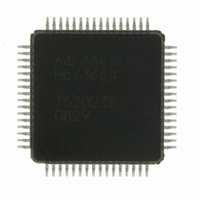
HD64F3664FPV
Manufacturer Part Number
HD64F3664FPV
Description
IC H8/3664 MCU FLASH 32K 64LQFP
Manufacturer
Renesas Electronics America
Series
H8® H8/300H Tinyr
Specifications of HD64F3664FPV
Core Size
16-Bit
Program Memory Size
32KB (32K x 8)
Oscillator Type
External
Core Processor
H8/300H
Speed
16MHz
Connectivity
I²C, SCI
Peripherals
PWM, WDT
Number Of I /o
29
Program Memory Type
FLASH
Ram Size
2K x 8
Voltage - Supply (vcc/vdd)
3 V ~ 5.5 V
Data Converters
A/D 8x10b
Operating Temperature
-20°C ~ 75°C
Package / Case
64-LQFP
No. Of I/o's
29
Ram Memory Size
2KB
Cpu Speed
16MHz
No. Of Timers
4
Digital Ic Case Style
LQFP
Supply Voltage
RoHS Compliant
Controller Family/series
H8/300H
Rohs Compliant
Yes
Lead Free Status / RoHS Status
Lead free / RoHS Compliant
Eeprom Size
-
Lead Free Status / RoHS Status
Lead free / RoHS Compliant
Available stocks
Company
Part Number
Manufacturer
Quantity
Price
Company:

Part Number:
HD64F3664FPV
Manufacturer:
MURATA
Quantity:
34 000
Company:
Part Number:
HD64F3664FPV
Manufacturer:
HD
Quantity:
465
Company:
Part Number:
HD64F3664FPV
Manufacturer:
Renesas Electronics America
Quantity:
10 000
Part Number:
HD64F3664FPV
Manufacturer:
RENESAS/瑞萨
Quantity:
20 000


14.8.2
When TE is 0, the TxD pin is used as an I/O port whose direction (input or output) and level are
determined by PCR and PDR. This can be used to set the TxD pin to mark state (high level) or
send a break during serial data transmission. To maintain the communication line at mark state
until TE is set to 1, set both PCR and PDR to 1. As TE is cleared to 0 at this point, the TxD pin
becomes an I/O port, and 1 is output from the TxD pin. To send a break during serial transmission,
first set PCR to 1 and PDR to 0, and then clear TE to 0. When TE is cleared to 0, the transmitter is
initialized regardless of the current transmission state, the TxD pin becomes an I/O port, and 0 is
output from the TxD pin.
14.8.3
Transmission cannot be started when a receive error flag (OER, PER, or FER) is set to 1, even if
the TDRE flag is cleared to 0. Be sure to clear the receive error flags to 0 before starting
transmission. Note also that receive error flags cannot be cleared to 0 even if the RE bit is cleared
to 0.
14.8.4
In asynchronous mode, the SCI3 operates on a basic clock with a frequency of 16 times the
transfer rate. In reception, the SCI3 samples the falling edge of the start bit using the basic clock,
and performs internal synchronization. Receive data is latched internally at the rising edge of the
8th pulse of the basic clock as shown in figure 14.19.
Thus, the reception margin in asynchronous mode is given by formula (1) below.
M = (0.5 –
Where N: Ratio of bit rate to clock (N = 16)
D: Clock duty (D = 0.5 to 1.0)
L: Frame length (L = 9 to 12)
F: Absolute value of clock rate deviation
Mark State and Break Sending
Receive Error Flags and Transmit Operations (Clocked Synchronous Mode Only)
Receive Data Sampling Timing and Reception Margin in Asynchronous Mode
2N
1
) –
D – 0.5
N
– (L – 0.5) F
100(%)
Section 14 Serial Communication Interface 3 (SCI3)
Rev. 6.00 Mar. 24, 2006 Page 231 of 412
... Formula (1)
REJ09B0142-0600
Related parts for HD64F3664FPV
Image
Part Number
Description
Manufacturer
Datasheet
Request
R


Part Number:
Description:
KIT STARTER FOR M16C/29
Manufacturer:
Renesas Electronics America
Datasheet:

Part Number:
Description:
KIT STARTER FOR R8C/2D
Manufacturer:
Renesas Electronics America
Datasheet:

Part Number:
Description:
R0K33062P STARTER KIT
Manufacturer:
Renesas Electronics America
Datasheet:

Part Number:
Description:
KIT STARTER FOR R8C/23 E8A
Manufacturer:
Renesas Electronics America
Datasheet:

Part Number:
Description:
KIT STARTER FOR R8C/25
Manufacturer:
Renesas Electronics America
Datasheet:

Part Number:
Description:
KIT STARTER H8S2456 SHARPE DSPLY
Manufacturer:
Renesas Electronics America
Datasheet:

Part Number:
Description:
KIT STARTER FOR R8C38C
Manufacturer:
Renesas Electronics America
Datasheet:

Part Number:
Description:
KIT STARTER FOR R8C35C
Manufacturer:
Renesas Electronics America
Datasheet:

Part Number:
Description:
KIT STARTER FOR R8CL3AC+LCD APPS
Manufacturer:
Renesas Electronics America
Datasheet:
Part Number:
Description:
KIT STARTER FOR RX610
Manufacturer:
Renesas Electronics America
Datasheet:

Part Number:
Description:
KIT STARTER FOR R32C/118
Manufacturer:
Renesas Electronics America
Datasheet:

Part Number:
Description:
KIT DEV RSK-R8C/26-29
Manufacturer:
Renesas Electronics America
Datasheet:

Part Number:
Description:
KIT STARTER FOR SH7124
Manufacturer:
Renesas Electronics America
Datasheet:

Part Number:
Description:
KIT STARTER FOR H8SX/1622
Manufacturer:
Renesas Electronics America
Datasheet: