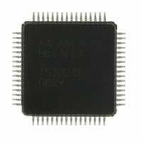
HD64F3664FPV Renesas Electronics America, HD64F3664FPV Datasheet - Page 313

HD64F3664FPV
Manufacturer Part Number
HD64F3664FPV
Description
IC H8/3664 MCU FLASH 32K 64LQFP
Manufacturer
Renesas Electronics America
Series
H8® H8/300H Tinyr
Specifications of HD64F3664FPV
Core Size
16-Bit
Program Memory Size
32KB (32K x 8)
Oscillator Type
External
Core Processor
H8/300H
Speed
16MHz
Connectivity
I²C, SCI
Peripherals
PWM, WDT
Number Of I /o
29
Program Memory Type
FLASH
Ram Size
2K x 8
Voltage - Supply (vcc/vdd)
3 V ~ 5.5 V
Data Converters
A/D 8x10b
Operating Temperature
-20°C ~ 75°C
Package / Case
64-LQFP
No. Of I/o's
29
Ram Memory Size
2KB
Cpu Speed
16MHz
No. Of Timers
4
Digital Ic Case Style
LQFP
Supply Voltage
RoHS Compliant
Controller Family/series
H8/300H
Rohs Compliant
Yes
Lead Free Status / RoHS Status
Lead free / RoHS Compliant
Eeprom Size
-
Lead Free Status / RoHS Status
Lead free / RoHS Compliant
Available stocks
Company
Part Number
Manufacturer
Quantity
Price
Company:
Part Number:
HD64F3664FPV
Manufacturer:
MURATA
Quantity:
34 000
Company:
Part Number:
HD64F3664FPV
Manufacturer:
HD
Quantity:
465
Company:
Part Number:
HD64F3664FPV
Manufacturer:
Renesas Electronics America
Quantity:
10 000
Part Number:
HD64F3664FPV
Manufacturer:
RENESAS/瑞萨
Quantity:
20 000
- Current page: 313 of 446
- Download datasheet (3Mb)
Table 16.3 A/D Conversion Time (Single Mode)
Note: All values represent the number of states.
16.4.4
The A/D conversion can also be started by an external trigger input. When the TRGE bit is set to 1
in ADCR, external trigger input is enabled at the ADTRG pin. A falling edge at the ADTRG
input pin sets the ADST bit to 1 in ADCSR, starting A/D conversion. Other operations, in both
single and scan modes, are the same as when the bit ADST has been set to 1 by software. Figure
16.3 shows the timing.
Item
A/D conversion start delay
Input sampling time
A/D conversion time
External Trigger Input Timing
ADTRG
Internal trigger
signal
ADST
Figure 16.3 External Trigger Input Timing
Symbol
t
t
t
D
SPL
CONV
Min
6
—
131
Typ
—
31
—
CKS = 0
A/D conversion
Rev. 6.00 Mar. 24, 2006 Page 283 of 412
Max
9
—
134
Min
4
—
69
Section 16 A/D Converter
CKS = 1
Typ
—
15
—
REJ09B0142-0600
Max
5
—
70
Related parts for HD64F3664FPV
Image
Part Number
Description
Manufacturer
Datasheet
Request
R

Part Number:
Description:
KIT STARTER FOR M16C/29
Manufacturer:
Renesas Electronics America
Datasheet:

Part Number:
Description:
KIT STARTER FOR R8C/2D
Manufacturer:
Renesas Electronics America
Datasheet:

Part Number:
Description:
R0K33062P STARTER KIT
Manufacturer:
Renesas Electronics America
Datasheet:

Part Number:
Description:
KIT STARTER FOR R8C/23 E8A
Manufacturer:
Renesas Electronics America
Datasheet:

Part Number:
Description:
KIT STARTER FOR R8C/25
Manufacturer:
Renesas Electronics America
Datasheet:

Part Number:
Description:
KIT STARTER H8S2456 SHARPE DSPLY
Manufacturer:
Renesas Electronics America
Datasheet:

Part Number:
Description:
KIT STARTER FOR R8C38C
Manufacturer:
Renesas Electronics America
Datasheet:

Part Number:
Description:
KIT STARTER FOR R8C35C
Manufacturer:
Renesas Electronics America
Datasheet:

Part Number:
Description:
KIT STARTER FOR R8CL3AC+LCD APPS
Manufacturer:
Renesas Electronics America
Datasheet:

Part Number:
Description:
KIT STARTER FOR RX610
Manufacturer:
Renesas Electronics America
Datasheet:

Part Number:
Description:
KIT STARTER FOR R32C/118
Manufacturer:
Renesas Electronics America
Datasheet:

Part Number:
Description:
KIT DEV RSK-R8C/26-29
Manufacturer:
Renesas Electronics America
Datasheet:

Part Number:
Description:
KIT STARTER FOR SH7124
Manufacturer:
Renesas Electronics America
Datasheet:

Part Number:
Description:
KIT STARTER FOR H8SX/1622
Manufacturer:
Renesas Electronics America
Datasheet:


