HD64F3664FPV Renesas Electronics America, HD64F3664FPV Datasheet - Page 395
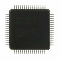
HD64F3664FPV
Manufacturer Part Number
HD64F3664FPV
Description
IC H8/3664 MCU FLASH 32K 64LQFP
Manufacturer
Renesas Electronics America
Series
H8® H8/300H Tinyr
Specifications of HD64F3664FPV
Core Size
16-Bit
Program Memory Size
32KB (32K x 8)
Oscillator Type
External
Core Processor
H8/300H
Speed
16MHz
Connectivity
I²C, SCI
Peripherals
PWM, WDT
Number Of I /o
29
Program Memory Type
FLASH
Ram Size
2K x 8
Voltage - Supply (vcc/vdd)
3 V ~ 5.5 V
Data Converters
A/D 8x10b
Operating Temperature
-20°C ~ 75°C
Package / Case
64-LQFP
No. Of I/o's
29
Ram Memory Size
2KB
Cpu Speed
16MHz
No. Of Timers
4
Digital Ic Case Style
LQFP
Supply Voltage
RoHS Compliant
Controller Family/series
H8/300H
Rohs Compliant
Yes
Lead Free Status / RoHS Status
Lead free / RoHS Compliant
Eeprom Size
-
Lead Free Status / RoHS Status
Lead free / RoHS Compliant
Available stocks
Company
Part Number
Manufacturer
Quantity
Price
Company:

Part Number:
HD64F3664FPV
Manufacturer:
MURATA
Quantity:
34 000
Company:
Part Number:
HD64F3664FPV
Manufacturer:
HD
Quantity:
465
Company:
Part Number:
HD64F3664FPV
Manufacturer:
Renesas Electronics America
Quantity:
10 000
Part Number:
HD64F3664FPV
Manufacturer:
RENESAS/瑞萨
Quantity:
20 000


A.3
The status of execution for each instruction of the H8/300H CPU and the method of calculating
the number of states required for instruction execution are shown below. Table A.4 shows the
number of cycles of each type occurring in each instruction, such as instruction fetch and data
read/write. Table A.3 shows the number of states required for each cycle. The total number of
states required for execution of an instruction can be calculated by the following expression:
Examples: When instruction is fetched from on-chip ROM, and an on-chip RAM is accessed.
From table A.4:
From table A.3:
Number of states required for execution = 2 × 2 + 2 × 2 = 8
When instruction is fetched from on-chip ROM, branch address is read from on-chip ROM, and
on-chip RAM is used for stack area.
From table A.4:
From table A.3:
Number of states required for execution = 2 × 2 + 1 × 2+ 1 × 2 = 8
BSET #0, @FF00
I = L = 2,
S
JSR @@ 30
I = 2,
S
I
I
= 2,
= S
Number of Execution States
Execution states = I × S
J
= S
J = K = 1,
S
K
L
= 2
= 2
J = K = M = N= 0
L = M = N = 0
I
+ J × S
J
+ K × S
K
+ L × S
L
+ M × S
Rev. 6.00 Mar. 24, 2006 Page 365 of 412
M
+ N × S
N
REJ09B0142-0600
Appendix
Related parts for HD64F3664FPV
Image
Part Number
Description
Manufacturer
Datasheet
Request
R


Part Number:
Description:
KIT STARTER FOR M16C/29
Manufacturer:
Renesas Electronics America
Datasheet:

Part Number:
Description:
KIT STARTER FOR R8C/2D
Manufacturer:
Renesas Electronics America
Datasheet:

Part Number:
Description:
R0K33062P STARTER KIT
Manufacturer:
Renesas Electronics America
Datasheet:

Part Number:
Description:
KIT STARTER FOR R8C/23 E8A
Manufacturer:
Renesas Electronics America
Datasheet:

Part Number:
Description:
KIT STARTER FOR R8C/25
Manufacturer:
Renesas Electronics America
Datasheet:

Part Number:
Description:
KIT STARTER H8S2456 SHARPE DSPLY
Manufacturer:
Renesas Electronics America
Datasheet:

Part Number:
Description:
KIT STARTER FOR R8C38C
Manufacturer:
Renesas Electronics America
Datasheet:

Part Number:
Description:
KIT STARTER FOR R8C35C
Manufacturer:
Renesas Electronics America
Datasheet:

Part Number:
Description:
KIT STARTER FOR R8CL3AC+LCD APPS
Manufacturer:
Renesas Electronics America
Datasheet:
Part Number:
Description:
KIT STARTER FOR RX610
Manufacturer:
Renesas Electronics America
Datasheet:

Part Number:
Description:
KIT STARTER FOR R32C/118
Manufacturer:
Renesas Electronics America
Datasheet:

Part Number:
Description:
KIT DEV RSK-R8C/26-29
Manufacturer:
Renesas Electronics America
Datasheet:

Part Number:
Description:
KIT STARTER FOR SH7124
Manufacturer:
Renesas Electronics America
Datasheet:

Part Number:
Description:
KIT STARTER FOR H8SX/1622
Manufacturer:
Renesas Electronics America
Datasheet: