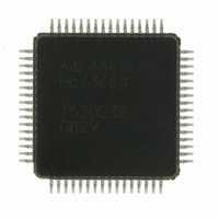
HD64F3664FPV Renesas Electronics America, HD64F3664FPV Datasheet - Page 296

HD64F3664FPV
Manufacturer Part Number
HD64F3664FPV
Description
IC H8/3664 MCU FLASH 32K 64LQFP
Manufacturer
Renesas Electronics America
Series
H8® H8/300H Tinyr
Specifications of HD64F3664FPV
Core Size
16-Bit
Program Memory Size
32KB (32K x 8)
Oscillator Type
External
Core Processor
H8/300H
Speed
16MHz
Connectivity
I²C, SCI
Peripherals
PWM, WDT
Number Of I /o
29
Program Memory Type
FLASH
Ram Size
2K x 8
Voltage - Supply (vcc/vdd)
3 V ~ 5.5 V
Data Converters
A/D 8x10b
Operating Temperature
-20°C ~ 75°C
Package / Case
64-LQFP
No. Of I/o's
29
Ram Memory Size
2KB
Cpu Speed
16MHz
No. Of Timers
4
Digital Ic Case Style
LQFP
Supply Voltage
RoHS Compliant
Controller Family/series
H8/300H
Rohs Compliant
Yes
Lead Free Status / RoHS Status
Lead free / RoHS Compliant
Eeprom Size
-
Lead Free Status / RoHS Status
Lead free / RoHS Compliant
Available stocks
Company
Part Number
Manufacturer
Quantity
Price
Company:
Part Number:
HD64F3664FPV
Manufacturer:
MURATA
Quantity:
34 000
Company:
Part Number:
HD64F3664FPV
Manufacturer:
HD
Quantity:
465
Company:
Part Number:
HD64F3664FPV
Manufacturer:
Renesas Electronics America
Quantity:
10 000
Part Number:
HD64F3664FPV
Manufacturer:
RENESAS/瑞萨
Quantity:
20 000
- Current page: 296 of 446
- Download datasheet (3Mb)
Section 15 I
15.5
1. In master mode, if an instruction to generate a start condition is immediately followed by an
2. Either of the following two conditions will start the next transfer. Pay attention to these
3. Table 15.5 shows the timing of SCL and SDA output in synchronization with the internal
Table 15.5 I
4. SCL and SDA inputs are sampled in synchronization with the internal clock. The AC timing
Rev. 6.00 Mar. 24, 2006 Page 266 of 412
REJ09B0142-0600
Item
SCL output cycle time
SCL output high pulse width
SCL output low pulse width
SDA output bus free time
Start condition output hold time
Retransmission start condition output
setup time
Stop condition output setup time
Data output setup time (master)
Data output setup time (slave)
Data output hold time
instruction to generate a stop condition, neither condition will be output correctly. To output
consecutive start and stop conditions, after issuing the instruction that generates the start
condition, read the relevant ports, check that SCL and SDA are both low, then issue the
instruction that generates the stop condition. Note that SCL may not yet have gone low when
BBSY is cleared to 0.
conditions when reading or writing to ICDR.
Write access to ICDR when ICE = 1 and TRS = 1 (including automatic transfer from
Read access to ICDR when ICE = 1 and TRS = 0 (including automatic transfer from
therefore depends on the system clock cycle t
Characteristics. Note that the I
system clock frequency of less than 5 MHz.
clock. Timings on the bus are determined by the rise and fall times of signals affected by the
bus load capacitance, series resistance, and parallel resistance.
ICDRT to ICDRS)
ICDRS to ICDRR)
Usage Notes
2
C Bus Interface (IIC)
2
C Bus Timing (SCL and SDA Output)
2
C bus interface AC timing specifications will not be met with a
Symbol
t
t
t
t
t
t
t
t
t
SCLO
SCLHO
SCLLO
BUFO
STAHO
STASO
STOSO
SDASO
SDAHO
cyc
, as shown in table 20-4 in section 20, Electrical
Output Timing
28t
0.5t
0.5t
0.5t
0.5t
1t
0.5t
1t
1t
3t
SCLO
SCLLO
SCLL
cyc
cyc
SCLO
SCLO
SCLO
SCLO
SCLO
– 3t
to 256t
– 3t
– 1t
– 1t
+ 2t
cyc
cyc
cyc
cyc
cyc
cyc
Unit
ns
ns
ns
ns
ns
ns
ns
ns
ns
ns
Notes
Related parts for HD64F3664FPV
Image
Part Number
Description
Manufacturer
Datasheet
Request
R

Part Number:
Description:
KIT STARTER FOR M16C/29
Manufacturer:
Renesas Electronics America
Datasheet:

Part Number:
Description:
KIT STARTER FOR R8C/2D
Manufacturer:
Renesas Electronics America
Datasheet:

Part Number:
Description:
R0K33062P STARTER KIT
Manufacturer:
Renesas Electronics America
Datasheet:

Part Number:
Description:
KIT STARTER FOR R8C/23 E8A
Manufacturer:
Renesas Electronics America
Datasheet:

Part Number:
Description:
KIT STARTER FOR R8C/25
Manufacturer:
Renesas Electronics America
Datasheet:

Part Number:
Description:
KIT STARTER H8S2456 SHARPE DSPLY
Manufacturer:
Renesas Electronics America
Datasheet:

Part Number:
Description:
KIT STARTER FOR R8C38C
Manufacturer:
Renesas Electronics America
Datasheet:

Part Number:
Description:
KIT STARTER FOR R8C35C
Manufacturer:
Renesas Electronics America
Datasheet:

Part Number:
Description:
KIT STARTER FOR R8CL3AC+LCD APPS
Manufacturer:
Renesas Electronics America
Datasheet:

Part Number:
Description:
KIT STARTER FOR RX610
Manufacturer:
Renesas Electronics America
Datasheet:

Part Number:
Description:
KIT STARTER FOR R32C/118
Manufacturer:
Renesas Electronics America
Datasheet:

Part Number:
Description:
KIT DEV RSK-R8C/26-29
Manufacturer:
Renesas Electronics America
Datasheet:

Part Number:
Description:
KIT STARTER FOR SH7124
Manufacturer:
Renesas Electronics America
Datasheet:

Part Number:
Description:
KIT STARTER FOR H8SX/1622
Manufacturer:
Renesas Electronics America
Datasheet:


