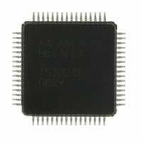
HD64F3664FPV Renesas Electronics America, HD64F3664FPV Datasheet - Page 434

HD64F3664FPV
Manufacturer Part Number
HD64F3664FPV
Description
IC H8/3664 MCU FLASH 32K 64LQFP
Manufacturer
Renesas Electronics America
Series
H8® H8/300H Tinyr
Specifications of HD64F3664FPV
Core Size
16-Bit
Program Memory Size
32KB (32K x 8)
Oscillator Type
External
Core Processor
H8/300H
Speed
16MHz
Connectivity
I²C, SCI
Peripherals
PWM, WDT
Number Of I /o
29
Program Memory Type
FLASH
Ram Size
2K x 8
Voltage - Supply (vcc/vdd)
3 V ~ 5.5 V
Data Converters
A/D 8x10b
Operating Temperature
-20°C ~ 75°C
Package / Case
64-LQFP
No. Of I/o's
29
Ram Memory Size
2KB
Cpu Speed
16MHz
No. Of Timers
4
Digital Ic Case Style
LQFP
Supply Voltage
RoHS Compliant
Controller Family/series
H8/300H
Rohs Compliant
Yes
Lead Free Status / RoHS Status
Lead free / RoHS Compliant
Eeprom Size
-
Lead Free Status / RoHS Status
Lead free / RoHS Compliant
Available stocks
Company
Part Number
Manufacturer
Quantity
Price
Company:
Part Number:
HD64F3664FPV
Manufacturer:
MURATA
Quantity:
34 000
Company:
Part Number:
HD64F3664FPV
Manufacturer:
HD
Quantity:
465
Company:
Part Number:
HD64F3664FPV
Manufacturer:
Renesas Electronics America
Quantity:
10 000
Part Number:
HD64F3664FPV
Manufacturer:
RENESAS/瑞萨
Quantity:
20 000
- Current page: 434 of 446
- Download datasheet (3Mb)
Rev. 6.00 Mar. 24, 2006 Page 404 of 412
REJ09B0142-0600
Item
6.1.1 System Control Register 1
(SYSCR1)
Table 7.2 Boot Mode Operation
9.5.3 Pin Functions
•
P84/FTIOD Pin
Page Revision (See Manual for Details)
85
102
136
Amended
Amended
Amended
Bit
3
Register
Bit Name
Setting Value
Transmits data H'55 when data H'00
Continuously transmits data H'00
Bit Name Description
NESEL
is received error-free.
at specified bit rate.
Processing Contents
Host Operation
TMRW
PWMD
0
1
Noise Elimination Sampling Frequency Select
The subclock pulse generator generates the watch
clock signal (φ
generator generates the oscillator clock (φ
bit selects the sampling frequency of the oscillator
clock when the watch clock signal (φ
When φ
0: Sampling rate is φ
1: Sampling rate is φ
IOD2
0
0
0
1
X
TIOR1
IOD1
0
0
1
X
X
OSC
Communication Contents
= 4 to 16 MHz, clear NESEL to 0.
H'00, H'00 . . . H'00
IOD0
0
1
X
X
X
W
) and the system clock pulse
H'00
H'55
PCR8
PCR84
0
1
X
X
0
1
X
OSC
OSC
/16
/4
• Measures low-level period of receive data
• Calculates bit rate and sets BRR in SCI3.
• Transmits data H'00 to host as adjustment
H'55 reception.
H'00.
end indication.
Pin Function
P84 input/FTIOD input pin
P84 output/FTIOD input pin
FTIOD output pin
FTIOD output pin
P84 input/FTIOD input pin
P84 output/FTIOD input pin
PWM output pin
Processing Contents
LSI Operation
W
) is sampled.
OSC
). This
Related parts for HD64F3664FPV
Image
Part Number
Description
Manufacturer
Datasheet
Request
R

Part Number:
Description:
KIT STARTER FOR M16C/29
Manufacturer:
Renesas Electronics America
Datasheet:

Part Number:
Description:
KIT STARTER FOR R8C/2D
Manufacturer:
Renesas Electronics America
Datasheet:

Part Number:
Description:
R0K33062P STARTER KIT
Manufacturer:
Renesas Electronics America
Datasheet:

Part Number:
Description:
KIT STARTER FOR R8C/23 E8A
Manufacturer:
Renesas Electronics America
Datasheet:

Part Number:
Description:
KIT STARTER FOR R8C/25
Manufacturer:
Renesas Electronics America
Datasheet:

Part Number:
Description:
KIT STARTER H8S2456 SHARPE DSPLY
Manufacturer:
Renesas Electronics America
Datasheet:

Part Number:
Description:
KIT STARTER FOR R8C38C
Manufacturer:
Renesas Electronics America
Datasheet:

Part Number:
Description:
KIT STARTER FOR R8C35C
Manufacturer:
Renesas Electronics America
Datasheet:

Part Number:
Description:
KIT STARTER FOR R8CL3AC+LCD APPS
Manufacturer:
Renesas Electronics America
Datasheet:

Part Number:
Description:
KIT STARTER FOR RX610
Manufacturer:
Renesas Electronics America
Datasheet:

Part Number:
Description:
KIT STARTER FOR R32C/118
Manufacturer:
Renesas Electronics America
Datasheet:

Part Number:
Description:
KIT DEV RSK-R8C/26-29
Manufacturer:
Renesas Electronics America
Datasheet:

Part Number:
Description:
KIT STARTER FOR SH7124
Manufacturer:
Renesas Electronics America
Datasheet:

Part Number:
Description:
KIT STARTER FOR H8SX/1622
Manufacturer:
Renesas Electronics America
Datasheet:


